To our customers, Old Company Name in Catalogs and Other Documents On April 1st, 2010, NEC Electronics Corporation merged with Renesas Technology Corporation, and Renesas Electronics Corporation took over all the business of both companies. Therefore, although the old company name remains in this document, it is a valid Renesas Electronics document. We appreciate your understanding. Renesas Electronics website: http://www.renesas.
Notice 1. 2. 3. 4. 5. 6. 7. All information included in this document is current as of the date this document is issued. Such information, however, is subject to change without any prior notice. Before purchasing or using any Renesas Electronics products listed herein, please confirm the latest product information with a Renesas Electronics sales office.
Under development This document is under development and its contents are subject to change M16C/6N Group (M16C/6NL, M16C/6NN) Renesas MCU REJ03B0061-0210 Rev.2.10 Aug 25, 2006 1. Overview The M16C/6N Group (M16C/6NL, M16C/6NN) of MCUs are built using the high-performance silicon gate CMOS process using the M16C/60 Series CPU core and are packaged in 100-pin and 128-pin plastic molded LQFP. These MCUs operate using sophisticated instructions featuring a high level of instruction efficiency.
Under development This document is under development and its contents are subject to change. M16C/6N Group (M16C/6NL, M16C/6NN) 1. Overview 1.2 Performance Overview Tables 1.1 and 1.2 list the Functions and Specifications for M16C/6N Group (M16C/6NL, M16C/6NN). Table 1.1 Functions and Specifications for M16C/6N Group (100-pin Version: M16C/6NL) Item Specification CPU 91 instructions Number of fundamental instructions Minimum instruction execution time 41.
Under development This document is under development and its contents are subject to change. M16C/6N Group (M16C/6NL, M16C/6NN) 1. Overview Table 1.
Under development This document is under development and its contents are subject to change. M16C/6N Group (M16C/6NL, M16C/6NN) 1. Overview 1.3 Block Diagram Figure 1.1 shows a Block Diagram. 8 Port P0 8 8 Port P1 Port P3 INTB PC Rev.2.10 Aug 25, 2006 REJ03B0061-0210 page 4 of 67 Port P13 (3) (3) 2 8 Port P12 (3) 8 Port P11 (3) 8 8 Figure 1.1 Block Diagram Multiplier FLG Port P14 NOTES: 1: ROM size depends on MCU type. 2: RAM size depends on MCU type.
Under development This document is under development and its contents are subject to change. M16C/6N Group (M16C/6NL, M16C/6NN) 1. Overview 1.4 Product Information Table 1.3 lists the Product Information and Figure 1.2 shows the Type Number, Memory Size, and Packages. Table 1.3 Product Information Type No. M306NLFHGP M306NNFHGP M306NLFJGP M306NNFJGP As of Aug.
Under development This document is under development and its contents are subject to change. M16C/6N Group (M16C/6NL, M16C/6NN) 1. Overview 1.
Under development This document is under development and its contents are subject to change. M16C/6N Group (M16C/6NL, M16C/6NN) 1. Overview Table 1.4 List of Pin Names for 100-Pin Package (1) Pin No.
Under development This document is under development and its contents are subject to change. M16C/6N Group (M16C/6NL, M16C/6NN) 1. Overview Table 1.5 List of Pin Names for 100-Pin Package (2) Pin No.
VREF AVCC P9_7/ADTRG/SIN4 P9_6/ANEX1/CTX0/SOUT4 P9_5/ANEX0/CRX0/CLK4 P9_4/DA1/TB4IN P9_3/DA0/TB3IN P9_2/TB2IN/SOUT3 (1) P9_1/TB1IN/SIN3 P9_0/TB0IN/CLK3 P14_1 P14_0 BYTE CNVSS P8_7/XCIN P8_6/XCOUT RESET XOUT VSS XIN VCC1 P8_5/NMI P8_4/INT2/ZP P8_3/INT1 P8_2/INT0 P8_1/TA4IN/U P8_0/TA4OUT/U(SIN4) P7_7/TA3IN P7_6/TA3OUT P7_5/TA2IN/W(SOUT4) P7_4/TA2OUT/W(CLK4) P7_3/CTS2/RTS2/TA1IN/V P7_2/CLK2/TA1OUT/V (1) P7_1/RXD2/SCL2/TA0IN/TB5IN P7_0/TXD2/SDA2/TA0OUT P6_7/TXD1/SDA1 VCC1 P6_6/RXD1/SCL1 Rev.2.
Under development This document is under development and its contents are subject to change. M16C/6N Group (M16C/6NL, M16C/6NN) 1. Overview Table 1.6 List of Pin Names for 128-Pin Package (1) Pin No.
Under development This document is under development and its contents are subject to change. M16C/6N Group (M16C/6NL, M16C/6NN) 1. Overview Table 1.7 List of Pin Names for 128-Pin Package (2) Pin No.
Under development This document is under development and its contents are subject to change. M16C/6N Group (M16C/6NL, M16C/6NN) 1. Overview Table 1.8 List of Pin Names for 128-Pin Package (3) Pin No.
Under development This document is under development and its contents are subject to change. M16C/6N Group (M16C/6NL, M16C/6NN) 1. Overview 1.6 Pin Functions Tables 1.9 to 1.11 list the Pin Functions. Table 1.9 Pin Functions (100-pin and 128-pin Versions) (1) Signal Name Power supply input Analog power supply input Reset input CNVSS Pin Name VCC1, VCC2, VSS AVCC, AVSS I/O Type Description I Apply 3.0 to 5.
Under development This document is under development and its contents are subject to change. M16C/6N Group (M16C/6NL, M16C/6NN) 1. Overview Table 1.
Under development This document is under development and its contents are subject to change. M16C/6N Group (M16C/6NL, M16C/6NN) 1. Overview Table 1.11 Pin Functions (100-pin and 128-pin Versions) (3) Signal Name I/O port Pin Name P0_0 to P0_7 I/O Type Description 8-bit I/O ports in CMOS, having a direction register to select I/O P1_0 to P1_7 an input or output. P2_0 to P2_7 Each pin is set as an input port or output port.
Under development This document is under development and its contents are subject to change. M16C/6N Group (M16C/6NL, M16C/6NN) 2. Central Processing Unit (CPU) 2. Central Processing Unit (CPU) Figure 2.1 shows the CPU Registers. The CPU has 13 registers. Of these, R0, R1, R2, R3, A0, A1, and FB configure a register bank. There are two register banks.
Under development This document is under development and its contents are subject to change. M16C/6N Group (M16C/6NL, M16C/6NN) 2. Central Processing Unit (CPU) 2.3 Frame Base Register (FB) FB is configured with 16 bits, and is used for FB relative addressing. 2.4 Interrupt Table Register (INTB) INTB is configured with 20 bits, indicating the start address of an interrupt vector table. 2.5 Program Counter (PC) PC is configured with 20 bits, indicating the address of an instruction to be executed. 2.
Under development This document is under development and its contents are subject to change. M16C/6N Group (M16C/6NL, M16C/6NN) 3. Memory 3. Memory Figure 3.1 shows a Memory Map. The address space extends the 1 Mbyte from address 00000h to FFFFFh. The internal ROM is allocated in a lower address direction beginning with address FFFFFh. For example, a 512-Kbyte internal ROM is allocated to the addresses from 80000h to FFFFFh.
Under development This document is under development and its contents are subject to change. M16C/6N Group (M16C/6NL, M16C/6NN) 4. Special Function Registers (SFRs) 4. Special Function Registers (SFRs) An SFR (Special Function Register) is a control register for a peripheral function. Tables 4.1 to 4.12 list the SFR Information. Table 4.
Under development This document is under development and its contents are subject to change. M16C/6N Group (M16C/6NL, M16C/6NN) 4. Special Function Registers (SFRs) Table 4.
Under development This document is under development and its contents are subject to change. M16C/6N Group (M16C/6NL, M16C/6NN) 4. Special Function Registers (SFRs) Table 4.
Under development This document is under development and its contents are subject to change. M16C/6N Group (M16C/6NL, M16C/6NN) 4. Special Function Registers (SFRs) Table 4.
Under development This document is under development and its contents are subject to change. M16C/6N Group (M16C/6NL, M16C/6NN) 4. Special Function Registers (SFRs) Table 4.
Under development This document is under development and its contents are subject to change. M16C/6N Group (M16C/6NL, M16C/6NN) 4. Special Function Registers (SFRs) Table 4.
Under development This document is under development and its contents are subject to change. M16C/6N Group (M16C/6NL, M16C/6NN) 4. Special Function Registers (SFRs) Table 4.
Under development This document is under development and its contents are subject to change. M16C/6N Group (M16C/6NL, M16C/6NN) 4. Special Function Registers (SFRs) Table 4.
Under development This document is under development and its contents are subject to change. M16C/6N Group (M16C/6NL, M16C/6NN) Table 4.
Under development This document is under development and its contents are subject to change. M16C/6N Group (M16C/6NL, M16C/6NN) 4. Special Function Registers (SFRs) Table 4.
Under development This document is under development and its contents are subject to change. M16C/6N Group (M16C/6NL, M16C/6NN) 4. Special Function Registers (SFRs) Table 4.
Under development This document is under development and its contents are subject to change. M16C/6N Group (M16C/6NL, M16C/6NN) 4. Special Function Registers (SFRs) Table 4.
Under development This document is under development and its contents are subject to change. M16C/6N Group (M16C/6NL, M16C/6NN) 5. Electric Characteristics 5. Electrical Characteristics Table 5.1 Absolute Maximum Ratings Condition Rated Value Unit VCC Supply voltage (VCC1 = VCC2) VCC = AVCC –0.3 to 6.5 V AVCC Analog supply voltage VCC = AVCC VI Input RESET, CNVSS, BYTE, voltage P0_0 to P0_7, P1_0 to P1_7, P2_0 to P2_7, Symbol Parameter –0.3 to 6.5 V –0.3 to VCC+0.3 V –0.3 to 6.
Under development This document is under development and its contents are subject to change. M16C/6N Group (M16C/6NL, M16C/6NN) 5. Electric Characteristics Table 5.2 Recommended Operating Conditions (1) Symbol VCC AVCC VSS AVSS VIH VIL Parameter (1) Min. 3.0 Supply voltage (VCC1 = VCC2) Analog supply voltage Supply voltage Analog supply voltage HIGH input P3_1 to P3_7, P4_0 to P4_7, P5_0 to P5_7, P6_0 to P6_7, 0.
Under development This document is under development and its contents are subject to change. M16C/6N Group (M16C/6NL, M16C/6NN) 5. Electric Characteristics Table 5.3 Recommended Operating Conditions (2) Symbol f(XIN) (1) Parameter Min. Main clock input oscillation No wait Mask ROM version VCC = 3.0 to 5.5 V frequency (2) (3) (4) Standard Max. Typ.
Under development This document is under development and its contents are subject to change. M16C/6N Group (M16C/6NL, M16C/6NN) Table 5.4 Electrical Characteristics (1) Symbol VOH HIGH output voltage 5.
Under development This document is under development and its contents are subject to change. M16C/6N Group (M16C/6NL, M16C/6NN) Table 5.5 Electrical Characteristics (2) Symbol ICC 5. Electric Characteristics (1) Parameter Power supply Measuring Condition In single-chip mode, Mask ROM current Min. f(BCLK) = 24 MHz, Standard Typ. Max. 19 33 Unit mA PLL operation, the output pins are (VCC = 3.0 to 5.
Under development This document is under development and its contents are subject to change. M16C/6N Group (M16C/6NL, M16C/6NN) 5. Electric Characteristics (1) Table 5.6 A/D Conversion Characteristics Symbol Parameter – Resolution INL Integral 10 bits Min. VREF = VCC VREF ANEX0, ANEX1 input, AN0 to AN7 input, Standard Typ. Max.
Under development This document is under development and its contents are subject to change. M16C/6N Group (M16C/6NL, M16C/6NN) 5. Electric Characteristics Table 5.8 Flash Memory Version Electrical Characteristics Parameter Symbol (1) Min. (2) Standard Typ. Max. 25 200 µs Unit - Programming and erasure endurance - Word program time (VCC = 5.0 V) - Lock bit program time 25 200 µs - Block erase time 4-Kbyte block 0.3 4 s (VCC = 5.0 V) 8-Kbyte block 0.3 4 s 32-Kbyte block 0.
Under development This document is under development and its contents are subject to change. M16C/6N Group (M16C/6NL, M16C/6NN) 5. Electric Characteristics Timing Requirements VCC (Referenced to VCC = 5 V, VSS = 0 V, at Topr = –40 to 85°C unless otherwise specified) =5V Table 5.
Under development This document is under development and its contents are subject to change. M16C/6N Group (M16C/6NL, M16C/6NN) 5. Electric Characteristics Timing Requirements VCC (Referenced to VCC = 5 V, VSS = 0 V, at Topr = –40 to 85°C unless otherwise specified) =5V Table 5.13 Timer A Input (Counter Input in Event Counter Mode) Parameter Symbol tc(TA) TAiIN input cycle time tw(TAH) TAiIN input HIGH pulse width tw(TAL) TAiIN input LOW pulse width Standard Min. Max.
Under development This document is under development and its contents are subject to change. M16C/6N Group (M16C/6NL, M16C/6NN) 5. Electric Characteristics Timing Requirements VCC (Referenced to VCC = 5 V, VSS = 0 V, at Topr = –40 to 85°C unless otherwise specified) =5V Table 5.
Under development This document is under development and its contents are subject to change. M16C/6N Group (M16C/6NL, M16C/6NN) 5. Electric Characteristics Switching Characteristics VCC (Referenced to VCC = 5 V, VSS = 0 V, at Topr = –40 to 85 °C unless otherwise specified) =5V Table 5.
Under development This document is under development and its contents are subject to change. M16C/6N Group (M16C/6NL, M16C/6NN) 5. Electric Characteristics Switching Characteristics VCC (Referenced to VCC = 5 V, VSS = 0 V, at Topr = –40 to 85 °C unless otherwise specified) =5V Table 5.
Under development This document is under development and its contents are subject to change. M16C/6N Group (M16C/6NL, M16C/6NN) 5. Electric Characteristics Switching Characteristics VCC (Referenced to VCC = 5 V, VSS = 0 V, at Topr = –40 to 85 °C unless otherwise specified) =5V Table 5.
Under development This document is under development and its contents are subject to change. M16C/6N Group (M16C/6NL, M16C/6NN) 5.
Under development This document is under development and its contents are subject to change. M16C/6N Group (M16C/6NL, M16C/6NN) 5.
Under development This document is under development and its contents are subject to change. M16C/6N Group (M16C/6NL, M16C/6NN) 5. Electric Characteristics Memory Expansion Mode and Microprocessor Mode (For setting with no wait) Read timing BCLK td(BCLK-CS) th(BCLK-CS) 25ns.max 4ns.min CSi tcyc td(BCLK-AD) th(BCLK-AD) 25ns.max 4ns.min ADi BHE td(BCLK-ALE) th(BCLK-ALE) -4ns.min 25ns.max th(RD-AD) 0ns.min ALE td(BCLK-RD) 25ns.max th(BCLK-RD) 0ns.min RD tac1(RD-DB) (0.5 ✕ tcyc-45)ns.
Under development This document is under development and its contents are subject to change. M16C/6N Group (M16C/6NL, M16C/6NN) 5. Electric Characteristics Memory Expansion Mode and Microprocessor Mode (For 1-wait setting and external area access) Read timing BCLK td(BCLK-CS) th(BCLK-CS) 25ns.max 4ns.min CSi tcyc td(BCLK-AD) th(BCLK-AD) 25ns.max 4ns.min ADi BHE td(BCLK-ALE) th(RD-AD) th(BCLK-ALE) 0ns.min -4ns.min 25ns.max ALE td(BCLK-RD) th(BCLK-RD) 0ns.min 25ns.max RD tac2(RD-DB) (1.
Under development This document is under development and its contents are subject to change. M16C/6N Group (M16C/6NL, M16C/6NN) 5. Electric Characteristics Memory Expansion Mode and Microprocessor Mode (For 2-wait setting and external area access) Read timing tcyc BCLK th(BCLK-CS) 4ns.min td(BCLK-CS) 25ns.max CSi th(BCLK-AD) 4ns.min td(BCLK-AD) 25ns.max ADi BHE td(BCLK-ALE) 25ns.max th(RD-AD) th(BCLK-ALE) -4ns.min 0ns.min ALE th(BCLK-RD) 0ns.min td(BCLK-RD) 25ns.max RD tac2(RD-DB) (2.
Under development This document is under development and its contents are subject to change. M16C/6N Group (M16C/6NL, M16C/6NN) 5. Electric Characteristics VCC = 5 V Memory Expansion Mode and Microprocessor Mode (For 3-wait setting and external area access) Read timing tcyc BCLK th(BCLK-CS) 4ns.min td(BCLK-CS) 25ns.max CSi th(BCLK-AD) td(BCLK-AD) 25ns.max 4ns.min ADi BHE td(BCLK-ALE) th(RD-AD) 0ns.min th(BCLK-ALE) 25ns.max -4ns.min ALE th(BCLK-RD) td(BCLK-RD) 25ns.max 0ns.
Under development This document is under development and its contents are subject to change. M16C/6N Group (M16C/6NL, M16C/6NN) 5. Electric Characteristics VCC = 5 V Memory Expansion Mode and Microprocessor Mode (For 1- or 2-wait setting, external area access and multiplexed bus selection) Read timing BCLK td(BCLK-CS) th(RD-CS) (0.5 ✕ tcyc-10)ns.min tcyc 25ns.max th(BCLK-CS) 4ns.min CSi td(AD-ALE) (0.5 ✕ tcyc-25)ns.min ADi /DBi th(ALE-AD) (0.5 ✕ tcyc-15)ns.min Address 8ns.
Under development This document is under development and its contents are subject to change. M16C/6N Group (M16C/6NL, M16C/6NN) 5. Electric Characteristics VCC = 5 V Memory Expansion Mode and Microprocessor Mode (For 3-wait setting, external area access and multiplexed bus selection) Read timing tcyc BCLK th(RD-CS) (0.5 ✕ tcyc-10)ns.min td(BCLK-CS) th(BCLK-CS) 4ns.min 25ns.max CSi td(AD-ALE) (0.5 ✕ tcyc-25)ns.min ADi /DBi th(ALE-AD) (0.5 ✕ tcyc-15)ns.min Address td(BCLK-AD) td(AD-RD) 25ns.
Under development This document is under development and its contents are subject to change. M16C/6N Group (M16C/6NL, M16C/6NN) Table 5.28 Electrical Characteristics 5. Electric Characteristics (1) VCC = 3.3 V Standard Parameter Measuring Condition Unit Symbol Min. Typ. Max. VCC P0_0 to P0_7, P1_0 to P1_7, P2_0 to P2_7, IOH = –1 mA V VOH HIGH output VCC-0.
Under development This document is under development and its contents are subject to change. M16C/6N Group (M16C/6NL, M16C/6NN) 5. Electric Characteristics Timing Requirements VCC (Referenced to VCC = 3.3 V, VSS = 0 V, at Topr = –40 to 85°C unless otherwise specified) = 3.3 V Table 5.
Under development This document is under development and its contents are subject to change. M16C/6N Group (M16C/6NL, M16C/6NN) 5. Electric Characteristics Timing Requirements VCC (Referenced to VCC = 3.3 V, VSS = 0 V, at Topr = –40 to 85°C unless otherwise specified) = 3.3 V Table 5.31 Timer A Input (Counter Input in Event Counter Mode) Parameter Symbol tc(TA) TAiIN input cycle time tw(TAH) TAiIN input HIGH pulse width tw(TAL) TAiIN input LOW pulse width Standard Min. Max.
Under development This document is under development and its contents are subject to change. M16C/6N Group (M16C/6NL, M16C/6NN) 5. Electric Characteristics Timing Requirements VCC (Referenced to VCC = 3.3 V, VSS = 0 V, at Topr = –40 to 85°C unless otherwise specified) = 3.3 V Table 5.
Under development This document is under development and its contents are subject to change. M16C/6N Group (M16C/6NL, M16C/6NN) 5. Electric Characteristics Switching Characteristics VCC (Referenced to VCC = 3.3 V, VSS = 0 V, at Topr = –40 to 85 °C unless otherwise specified) = 3.3 V Table 5.
Under development This document is under development and its contents are subject to change. M16C/6N Group (M16C/6NL, M16C/6NN) 5. Electric Characteristics Switching Characteristics VCC (Referenced to VCC = 3.3 V, VSS = 0 V, at Topr = –40 to 85 °C unless otherwise specified) = 3.3 V Table 5.
Under development This document is under development and its contents are subject to change. M16C/6N Group (M16C/6NL, M16C/6NN) 5. Electric Characteristics Switching Characteristics VCC (Referenced to VCC = 3.3 V, VSS = 0 V, at Topr = –40 to 85 °C unless otherwise specified) = 3.3 V Table 5.
Under development This document is under development and its contents are subject to change. M16C/6N Group (M16C/6NL, M16C/6NN) 5. Electric Characteristics VCC = 3.
Under development This document is under development and its contents are subject to change. M16C/6N Group (M16C/6NL, M16C/6NN) 5. Electric Characteristics Memory Expansion Mode and Microprocessor Mode VCC = 3.
Under development This document is under development and its contents are subject to change. M16C/6N Group (M16C/6NL, M16C/6NN) 5. Electric Characteristics Memory Expansion Mode and Microprocessor Mode (For setting with no wait) Read timing BCLK td(BCLK-CS) th(BCLK-CS) 30ns.max 4ns.min CSi tcyc td(BCLK-AD) th(BCLK-AD) 30ns.max 4ns.min ADi BHE td(BCLK-ALE) th(BCLK-ALE) -4ns.min 30ns.max th(RD-AD) 0ns.min ALE td(BCLK-RD) 30ns.max th(BCLK-RD) 0ns.min RD tac1(RD-DB) (0.5 ✕ tcyc-60)ns.
Under development This document is under development and its contents are subject to change. M16C/6N Group (M16C/6NL, M16C/6NN) 5. Electric Characteristics Memory Expansion Mode and Microprocessor Mode (For 1-wait setting and external area access) Read timing BCLK td(BCLK-CS) th(BCLK-CS) 30ns.max 4ns.min CSi tcyc td(BCLK-AD) th(BCLK-AD) 30ns.max 4ns.min ADi BHE td(BCLK-ALE) th(RD-AD) th(BCLK-ALE) 0ns.min -4ns.min 30ns.max ALE td(BCLK-RD) th(BCLK-RD) 0ns.min 30ns.max RD tac2(RD-DB) (1.
Under development This document is under development and its contents are subject to change. M16C/6N Group (M16C/6NL, M16C/6NN) 5. Electric Characteristics Memory Expansion Mode and Microprocessor Mode (For 2-wait setting and external area access) Read timing tcyc BCLK th(BCLK-CS) 4ns.min td(BCLK-CS) 30ns.max CSi th(BCLK-AD) 4ns.min td(BCLK-AD) 30ns.max ADi BHE td(BCLK-ALE) 30ns.max th(RD-AD) th(BCLK-ALE) -4ns.min 0ns.min ALE th(BCLK-RD) 0ns.min td(BCLK-RD) 30ns.max RD tac2(RD-DB) (2.
Under development This document is under development and its contents are subject to change. M16C/6N Group (M16C/6NL, M16C/6NN) 5. Electric Characteristics VCC = 3.3 V Memory Expansion Mode and Microprocessor Mode (For 3-wait setting and external area access) Read timing tcyc BCLK th(BCLK-CS) 4ns.min td(BCLK-CS) 30ns.max CSi th(BCLK-AD) td(BCLK-AD) 30ns.max 4ns.min ADi BHE td(BCLK-ALE) th(RD-AD) 0ns.min th(BCLK-ALE) 30ns.max -4ns.min ALE th(BCLK-RD) td(BCLK-RD) 30ns.max 0ns.
Under development This document is under development and its contents are subject to change. M16C/6N Group (M16C/6NL, M16C/6NN) 5. Electric Characteristics VCC = 3.3 V Memory Expansion Mode and Microprocessor Mode (For 2-wait setting, external area access and multiplexed bus selection) Read timing BCLK td(BCLK-CS) th(RD-CS) (0.5 ✕ tcyc-10)ns.min tcyc 40ns.max th(BCLK-CS) 4ns.min CSi td(AD-ALE) (0.5 ✕ tcyc-40)ns.min ADi /DBi Address th(ALE-AD) (0.5 ✕ tcyc-15)ns.min 8ns.
Under development This document is under development and its contents are subject to change. M16C/6N Group (M16C/6NL, M16C/6NN) 5. Electric Characteristics Memory Expansion Mode and Microprocessor Mode VCC = 3.3 V (For 3-wait setting, external area access and multiplexed bus selection) Read timing tcyc BCLK th(RD-CS) (0.5 ✕ tcyc-10)ns.min td(BCLK-CS) th(BCLK-CS) 6ns.min 40ns.max CSi td(AD-ALE) (0.5 ✕ tcyc-40)ns.min ADi /DBi th(ALE-AD) (0.5 ✕ tcyc-15)ns.min Address td(BCLK-AD) td(AD-RD) 40ns.
Under development This document is under development and its contents are subject to change. M16C/6N Group (M16C/6NL, M16C/6NN) Appendix 1. Package Dimensions Appendix 1. Package Dimensions JEITA Package Code P-LQFP100-14x14-0.50 RENESAS Code PLQP0100KB-A Previous Code 100P6Q-A / FP-100U / FP-100UV MASS[Typ.] 0.6g HD *1 D 51 75 NOTE) 1. DIMENSIONS "*1" AND "*2" DO NOT INCLUDE MOLD FLASH. 2. DIMENSION "*3" DOES NOT INCLUDE TRIM OFFSET.
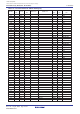
REVISION HISTORY Rev. Date M16C/6N Group (M16C/6NL, M16C/6NN) Data Sheet Description Page Summary 1.00 Jul. 20, 2004 – First edition issued 1.01 Nov. 01, 2004 – Revised edition issued * Revised parts and revised contents are as follows (except for expressional change). 26 Table 5.2 Recommended Operating Conditions (1) • IOH(peak): Unit is revised from “V” to “mA”. 27 Table 5.3 Recommended Operating Conditions (2) 28 Table 5.4 IIH, IIL: “P3_3” is revised to “P3_7” in Parameter. 31 Table 5.
REVISION HISTORY Rev. Date 2.10 Aug.25, 2006 M16C/6N Group (M16C/6NL, M16C/6NN) Data Sheet Description Page 26 Summary Table 4.8 SFR Information (8) • The value of After Reset in IDB0 register is revised. • The value of After Reset in IDB1 register is revised. 30 Table 4.12 SFR Information (12) • Value of After Reset in PUR1 is revised. • NOTE 1 is added. 32 Table 5.2 Recommended Operating Conditions (1) is partly revised. 33 Table 5.
Sales Strategic Planning Div. Nippon Bldg., 2-6-2, Ohte-machi, Chiyoda-ku, Tokyo 100-0004, Japan Keep safety first in your circuit designs! 1. Renesas Technology Corp. puts the maximum effort into making semiconductor products better and more reliable, but there is always the possibility that trouble may occur with them. Trouble with semiconductors may lead to personal injury, fire or property damage.