M306H2T-RPD-E Emulation Pod for M16C/6H Group M306H2 User's Manual Rev.1.
* NQPACK, YAPACK, YQSOCKET, YQ-Guide, HQPACK, TQPACK, and TQSOCKET are trademarks of Tokyo Eletech Corporation. Keep safety first in your circuit designs! • Renesas Technology Corporation and Renesas Solutions Corporation put the maximum effort into making semiconductor products better and more reliable, but there is always the possibility that trouble may occur with them. Trouble with semiconductors may lead to personal injury, fire or property damage.
Preface The M306H2T-RPD-E is an emulation pod for M306H2 of M16C/6H Group of 16-bit MCUs. It is used with a PC4701 emulator. This user's manual mainly describes specifications of the M306H2T-RPD-E emulation pod and how to setup it. For details on the following products, which are used with M306H2T-RPD-E, refer to each product's user's manual. • Emulator: • Emulator debugger: PC4701 User's Manual Emulator debugger for PC4701 series User's Manual All the components of this product are shown in "2.
Contents Chapter 1. Precautions for Safety ........................................................................................... 7 1.1 Safety Symbols and Meanings .............................................................................. 9 Chapter 2. Preparation .......................................................................................................... 21 2.1 Terminology ........................................................................................................ 22 2.
Chapter 5. Specifications ...................................................................................................... 51 5.1 Specifications ...................................................................................................... 52 5.2 Operation Timing in the Memory Expansion and Microprocessor Modes (5 V) ... 53 (1) Separate Bus, No-wait .............................................................................. 53 (2) Separate Bus, With Wait, Accessing External Memory Area ....
MEMO ( 6 / 76 )
Chapter 1. Precautions for Safety This chapter describes precautions for using this product safely and properly. For precautions for the emulator main unit and the emulator debugger, refer to each user's manual included with your product. 1.1 Safety Symbols and Meanings ..................................................................................................... 9 WARNING Warning for Installation .............................................................................................
Notes on Pullup Control Resistor .............................................................................. 16 Note on Reading Internal Resources of an MCU ...................................................... 16 Notes on Watchdog Function..................................................................................... 16 Note on Differences between Actual MCUs and the Emulator .................................
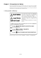
Chapter 1. Precautions for Safety In both the User's Manual and on the product itself, several icons are used to insure proper handling of this product and also to prevent injuries to you or other persons, or damage to your properties. This chapter describes the precautions which should be taken in order to use this product safely and properly. Be sure to read this chapter before using this product. 1.
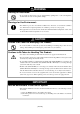
WARNING Warning for Installation: • Do not set this product in water or areas of high humidity. Spilling water or some other liquid into the main unit can cause an unrepairable damage. Warnings for Use Environment: • The emulation pod is air-cooled with the ventilation slot. Therefore, do not block the ventilation slot. When heated to high temperatures, the emulation pod may not work properly. • This equipment is to be used in an environment with a maximum ambient temperature of 35°C.
IMPORTANT Notes on Downloading Firmware: • Before using this product for the first time, it is necessary to download the dedicated firmware (control software for the emulation pod built into the PC4701). Please note that, to do this, it is necessary to start up the PC4701 in the maintenance mode. For firmware download procedures, see "4.2 Downloading Firmware" (page 48). Once the firmware has been downloaded, the product can be used by simply turning on the power.
IMPORTANT Notes on MAP References and Settings: • For details on referencing and setting MAP information, see user's manual of the emulator debugger. • Be sure to set the SFR area to EXTERNAL (an external section). • When setting 0FFFCh - 0FFFFh to EXTERNAL: This product uses the 4 bytes area 0FFFCh - 0FFFFh as the stack area. If this 4 bytes memory cannot be read or written to, reset cannot be properly effected. As a result, you need to alter the map settings if either of the conditions given below is met.
IMPORTANT Note on RESET* Input: • The RESET* input from the target system is accepted only while a user program is being executed (only while the RUN status LED on the PC4701's front panel is lit). Note on HOLD* Input: • Be sure to input "L" to the HOLD* pin of the target system during the user program execution (while the RUN status LED on the PC4701's front panel is lit). Inputting "L" to the HOLD* pin when stopping the user program may cause a malfunction of the emulator.
IMPORTANT Notes on Interruption: • Even when the target program is not being executed (while the target program is stopped or during runtime debugging), the evaluation MCU keeps running so as to control the emulation pod. Therefore, note that timers and other components do not stop running even though the target program is not being executed.
IMPORTANT Note on Commands that Access the Single-step Interrupt Vector Area: • Do not perform the following debugging operations with the single step interrupt vector area (addresses FFFECh - FFFEFh).
IMPORTANT Notes on Pullup Control Resistor: • Ports P00 to P57 are not pulled up by the pullup control resistor. When pulling up the ports P00 to P57, apply a resistance to the inside of the emulator. How to apply it, refer to "3.2 Setting Switches and Pullup Resistors" (page 29). Note: Ports P60 to P107 are pulled up by the pullup control resistors. Note: The pullup control resistors can read and write from P00 to P107 properly.
IMPORTANT Note on Differences between Actual MCUs and the Emulator: • Operations of the emulator system differ from those of actual MCUs as listed below. (1) Reset condition Set the rise time (0.2 Vcc to 0.8 Vcc) 1 µs or less. (2) Initial values of MCU's internal resources (3) Internal memories (ROM and RAM) capacities etc. With this emulator system, "INT" (emulation memory ON) is the default for mapping areas other than the SFR area (addresses 000h - 3FFh).
IMPORTANT Table 1.
IMPORTANT Table 1.4 Differences of outputs between actual MCUs and this product (in stop mode) Access area - Signal Actual MCU This product Address BHE* Retains previous status Retains previous status Data Retains previous status Floating RD* WR* Does not output (fixed to "H" output) Does not output (fixed to "H" output) CS* Retains previous status Retains previous status ALE Does not output (fixed to "H" output) Does not output (fixed to "H" output) ∗ for difference ∗ Table 1.
MEMO ( 20 / 76 )
Chapter 2. Preparation This chapter describes the package components, the system configuration and the preparation for using this product for the first time. 2.1 Terminology ............................................................................................................................... 22 2.2 Package Components.................................................................................................................. 23 2.3 Other Tool Products Required for Development.................
Chapter 2. Preparation 2.1 Terminology Some specific words used in this user's manual are defined as follows: Emulator system This means an emulator system built around the PC4701 emulator. The PC4701 emulator system is configured with an emulator main unit, emulation pod, host machine and emulator debugger. Emulator main unit (Hereafter PC4701) This means a generic name for emulators for 8 and 16-bit MCUs. For details on specific models of PC4701, visit the Renesas Tools Homepage. http://www.renesas.
2.2 Package Components The M306H2T-RPD-E package consists of the following items. When unpacking, check to see if your M306H2T-RPD-E contains all of these items.
2.4 Name of Each Part (1) System Configuration Figure 2.1 System configuration (1) to (4) in Figure 2.1 are included with this product package. (1) Emulation pod (M306H2T-RPD-E) This emulation pod contains an evaluation MCU, emulation memory and circuits to feature the debugging functions. (2) Flexible cable (FLX120-RPD) This is a 120-pin flexible cable for connecting the PC4701 emulator and the emulation pod.
(2) Inside of the Emulation Pod Figure 2.2 Internal view of the emulation pod (1) MCU-dependent boards 1 and 2 Boards grouping parts (pins and added functions) which vary according to MCU model. (2) Base board Board for the M16C/60 and M16C/20 Series MCUs which controls the interface with the PC4701 and the evaluation MCU. (3) Memory board Board on which is mounted the emulation memory (1 MB) and the map memory (4 bit×1M) for the M16C/60 and M16C/20 Series MCUs.
2.5 When Using the Emulator for the First Time If you have purchased this emulation pod newly, it is necessary to download the firmware. The download procedure is given in Figure 2.3. Before downloading the firmware, check the emulator debugger is installed and the PC4701 is connected to the host machine. For more information, see each user's manual of the emulator debugger and the PC4701. Connect the PC4701 and this product.
Chapter 3. Setting Up This chapter describes switch settings required for using this product and how to connect this product to the PC4701 and the target system. 3.1 Removing the Upper Cover ........................................................................................................ 28 3.2 Setting Switches and Pullup Resistors ....................................................................................... 29 3.3 Selecting Clock Supply ...................................................
Chapter 3. Setting Up To use this emulation pod with your target system, it is necessary to set as follows. Set the following after removing the upper cover. • Change the oscillation frequency in the emulation pod. • Set the switches depending on the target system. • Install pullup resistors to ports P00 to P57. • Install the A-D conversion bypass capacitor. • Change the input frequency for FSC oscillation. • Change the constant of the circuit for data slicer I/O signal. 3.
3.2 Setting Switches and Pullup Resistors Figure 3.2 shows the positions of switches and a position for installing pullup resistors. Tables 3.1 to 3.4 list how to set each switch and Figure 3.3 shows how to install pullup resistors. Figure 3.
Table 3.1 Switch settings of the M306H2T-RPD-E (1/4) Switch Signal Setting Description 16 OPEN 8 Pulls up the BYTE pin of MCU with a resistance at 33 kΩ. SW1 BYTE 16 OPEN SW1 BYTE 8 Does not pull down/up the BYTE pin of MCU. SW1 BYTE 16 OPEN 8 Pulls down the BYTE pin of MCU with a resistance at 33 kΩ. SW1 BYTE (Factory-setting) H OPEN L Pulls down the CNVSS pin of MCU with a resistance at 33 kΩ. SW2 CNVSS (Factory-setting) H SW2 OPEN CNVSS Does not pull down/up the CNVSS pin of MCU.
Table 3.2 Switch settings of the M306H2T-RPD-E (2/4) Switch Signal Setting Description XCIN P87 SW4 P87/XCIN Connects the P87/XCIN pin of MCU to the target system. (Uses P87/XCIN pin as port P87) SW4 P87/XCIN (Factory-setting) XCIN Uses P87/XCIN pin as XCIN. P87 SW4 P87/CIN XCOUT OPEN P86 Connects the P86/XCOUT pin of MCU to the target system.
Table 3.3 Switch settings of the M306H2T-RPD-E (3/4) Switch Signal Jumper switch setting SYNC/HOR SYNC/HOR JC1 SW6 FLX JC1 FLX SYNCIN Connects the SYNCIN pin to the Connects the SYNCIN pin to the RCA connector JC1 on the M306H0T- target system via the FLX160. PRT. (Factory-setting) JC2 SW7 Unused SW8 Unused FLX JC2 FLX Only this setting is available. Do not use this setting. (Factory-setting) JC3 FLX JC3 FLX Only this setting is available. Do not use this setting.
Table 3.4 Switch settings of the M306H2T-RPD-E (4/4) Switch Signal Jumper switch setting VR4 VREF1 SW11 VR4 VREF1 SVREF FLX FLX Connects the SVREF pin to the Connects the SVREF pin to the changeable resistance VR4 on the target system via the FLX160. M306H0T-PRT. (Factory-setting) SW12 JC4 JC4 FLX FLX Unused Only this setting is available. Do not use this setting. (Factory-setting) 4.43 MHz FSCIN FSCIN SW13 4.
It is not possible to control the pullup by the pullup control resistors of ports P00 to P57 (possible to read and write by the pullup control resistors). However, as this product has sockets for installing the pullup resistors, it is possible to pull up by mounting the resistor arrays included with this product. For the positions for installing the pullup resistors, see Figure 3.3. Figure 3.
3.3 Selecting Clock Supply There are two ways to supply a clock to the MCU, using the oscillator circuit of the emulation pod or using the oscillator circuit on the target system. Table 3.5 lists the factory-settings of each clock supply. Table 3.5 Clock supply to the MCU Clock Description Display of emulator debugger Default setting Internal oscillator circuit of emulation pod (OSC-3: 10 MHz) Internal Yes Target system External - Internal oscillator circuit of emulation pod (OSC-2: 32.
(1) Using the Oscillator Circuit on the Target System When turning on the power supply, the internal clock of emulation pod is selected to supply the clock to the MCU. To use the external clock on the target system, change the clock by the Init dialog when starting up the emulator debugger or the CLK command on the script window. (For details, refer to the user's manual (or online manual) of the emulator debugger) Figure 3.4 External oscillator circuit Figure 3.
(2) Changing the Internal Oscillator Circuit of the Emulation Pod An oscillator circuit board (OSC-3) for 10 MHz is mounted on this product. To use the emulation pod at a frequency other than 10 MHz, build the desired oscillator circuit on the included OSC-2 oscillator circuit board (bare board) and replace the board installed in the emulation pod when shipped from the factory. Figure 3.6 shows a view of the OSC-2 oscillator circuit board (bare board) and where connector pins are located. Figure 3.
(3) Replacing the Oscillator Circuit Boards Figure 3.8 shows how to replace the oscillator circuit boards. For the position of the oscillator circuit board, see Figure 3.2. (1) Unscrew the screw securing the oscillator circuit board. (2) Lift off the oscillator circuit board. (3) Attach the J1 connector of another oscillator circuit board for replacement to the connector of the MCU-dependent board. (4) Secure the oscillator circuit board with the screw. Figure 3.
3.4 A-D Conversion Bypass Capacitor With this product, there is a socket (0.1 µF pre-mounted) on the board for changing the bypass capacitor for the A-D conversion circuit. Remove or replace a suitable bypass capacitor as occasion demands. Figure 3.9 shows where the bypass capacitors are mounted, whereas Figure 3.10 shows an enlargement of the foot patterns. I/O signal circuit for data slicer Position to install the bypass capacitor for A-D converter Figure 3.
3.5 Data Slicer I/O Signal and FSC Clock I/O Signal Circuit With this product, the parts which are used for the data slicer and the FSC clock circuit are connected by sockets to be changed. Figure 3.11 shows the position of each part which is used for the data slicer and the FSC clock circuit. Figure 3.2 shows the layout of the parts and Figure 3.12 shows its detailed layout. Figure 3.11 Data slicer and FSC clock circuit Figure 3.
3.6 Connecting the PC4701 To connect the emulation pod to the PC4701, use the FLX120-RPD 120-pin flexible cable included with this product package. Connect the PC4701 side connector of the FLX120-RPD to the cable connector of the PC4701, then secure with screws the FLX120-RPD. (1) Connecting the Cable to the PC4701 Figure 3.13 shows how to connect the PC4701 and FLX120-RPD Figure 3.
(2) Connecting the Cable to the Emulation Pod Figure 3.14 shows how to connect the FLX120-RPD and the emulation pod. Figure 3.14 Connecting FLX120-RPD and emulation pod CAUTION Note on Connecting the Cable: • Always shut OFF power before connecting the cable. The power ON state could destroy internal circuits. Note on Securing the Screws: • After connecting the cable to the emulation pod, be sure to secure the screws.
3.7 Connecting the Target System Figure 3.15 shows how to connect the M306H2T-RPD-E and the target system. Figure 3.15 Connecting the emulation pod and the target system CAUTION Notes on Connecting the Target System: • Take care not to attach the converter board in a wrong direction. It may cause a fatal damage to the emulation pod. • The small connector of the M306H2T-PTC is guaranteed for only 50 insertion/ removal iterations.
3.8 Making an MCU File for PD30 It is necessary to change the contents of the MCU file according to the MCU to be developed. Make the MCU file "M306H2.MCU" for M306H2 and store it in the "mcufile" folder in the directory same as emulator debugger PD30 is stored. The contents of the MCU file (the SFR area, internal RAM area, internal ROM area, the name of the firmware file) are shown below. Change the settings according to the MCU to be debugged.
Chapter 4. Usage This chapter describes from turning on the power of this product to starting up the emulator debugger. 4.1 Turning On the Power ................................................................................................................ 46 (1) Checking the Connection of the Emulator System ............................................................... 46 (2) Turning On the Power...........................................................................................................
Chapter 4. Usage 4.1 Turning On the Power (1) Checking the Connection of the Emulator System Before turning the power ON, check the connection of the PC4701, emulation pod, converter board and target system. (2) Turning On the Power Power ON/OFF the target system and the PC4701 as simultaneously as possible. CAUTION Notes on Power Supply: • The emulator's VCC pin is connected to the target system in order to monitor target system voltage.
(3) LED Display When PC4701 Starts Up Normally After the emulator starts up, check the status of the LEDs on the front panel to see whether emulation pod operation is enabled or not. Figure 4.1 shows front panel LED lighting status when the emulator is turned ON. Figure 4.
4.2 Downloading Firmware (1) When It is Necessary to Download Firmware It is necessary to download the firmware when: (1) you use this product for the first time (2) the firmware has been upgraded (3) the emulator debugger has been upgraded (4) you use this product with a PC4701 which was used with other emulation pod before (2) Downloading Firmware in the Maintenance Mode Download the firmware in the maintenance mode as explained here following.
4.3 Self-checks (1) Self-check Procedure To run the emulator self-checks, do so as explained here below. While self-checks are in progress, LEDs will change as shown in Figure 4.4. (1) Set the switches in the emulation pod same as the factory setting (see Figure 4.3). (2) When the target system is connected, disconnect the target system. (3) Within 2 seconds of activating power to the emulator, press the RESET switch on the emulator front panel to switch the emulator to the maintenance mode.
Figure 4.
Chapter 5. Specifications This chapter describes specifications of this product. 5.1 Specifications ............................................................................................................................. 52 5.2 Operation Timing in the Memory Expansion and Microprocessor Modes (5 V) ...................... 53 (1) Separate Bus, No-wait ..........................................................................................................
Chapter 5. Specifications 5.1 Specifications Table 5.1 lists the specifications of the M306H2T-RPD-E. Table 5.1 Specifications of the M306H2T-RPD-E Emulators PC4701 Applicable MCUs M16C/6H Group M306H2 Evaluation MCU M30622SAFP, M306H2MC-TOOL Usable modes Single-chip mode Memory expansion mode Microprocessor mode Emulation memory 1 MB Maximum operating frequency 10 MHz Clock supply XIN-XOUT Internal oscillator circuit board (OSC-3) Switchable to external oscillator input.
5.2 Operation Timing in the Memory Expansion and Microprocessor Modes (5 V) (1) Separate Bus, No-Wait Table 5.2 and Figure 5.1 show the bus timing in the memory expansion and microprocessor modes (separate bus, no-wait). Table 5.2 Memory expansion and microprocessor modes (separate bus, no-wait) Symbol Item Actual MCU This product [ns] [ns] Min. Max. Min.
Memory expansion and microprocessor modes (no-wait) Read timing BCLK CSi ADi BHE ALE RD DB Write timing BCLK CSi ADi BHE ALE WR, WRL, WRH DB Conditions: • VCC = 5 V • Input timing voltage: VIL = 0.8 V, VIH = 2.5 V • Output timing voltage: VOL = 0.8 V, VOH = 2.0 V Figure 5.
(2) Separate Bus, With Wait, Accessing External Memory Area Table 5.3 and Figure 5.2 show the bus timing in the memory expansion and microprocessor modes (with wait, accessing external memory area). Table 5.3 Memory expansion and microprocessor modes (with wait, external memory area) Symbol Item Actual MCU This product [ns] [ns] Min. Max. Min.
Memory expansion and microprocessor modes (with wait, accessing external memory area) Read timing BCLK CSi ADi BHE ALE RD DB Write timing BCLK CSi ADi BHE ALE WR, WRL, WRH DB Conditions: • VCC = 5 V • Input timing voltage: VIL = 0.8 V, VIH = 2.5 V • Output timing voltage: VOL = 0.8 V, VOH = 2.0 V Figure 5.
(3) Multiplex Bus, With Wait, Accessing External Memory Area Table 5.4 and Figure 5.3 show the bus timing in the memory expansion and microprocessor modes (with wait, accessing external memory area and using multiplex bus). Table 5.4 Memory expansion and microprocessor modes (with wait, multiplex bus) Symbol Actual MCU This product [ns] [ns] Item Min. Td (BCLK-AD) Address output delay time Th (BCLK-AD) Address output hold time (BCLK standard) Th (RD-AD) Max. Min.
Memory expansion and microprocessor modes (with wait, accessing external memory area and using multiplex bus) Read timing BCLK CSi ADi DBi ADi BHE ALE WR Write timing BCLK CSi ADi DBi ADi BHE ALE WR, WRL, WRH Conditions: • VCC = 5 V • Input timing voltage: VIL = 0.8 V, VIH = 2.5 V • Output timing voltage: VOL = 0.8 V, VOH = 2.0 V Figure 5.
(4) Timing Requirements Table 5.5, Figures 5.4 and 5.5 show timing requirements in the memory expansion and microprocessor modes. Table 5.5 Timing requirements (VCC = 5 V) Symbol Actual MCU This product [ns] [ns] Item Min. Tsu (DB-RD) Data input setup time Max. Min.
Common to "with wait" and "no-wait" (actual MCU) BCLK HOLD input HLDA output P0, P1, P2, P3, P4, P50 to P52 Common to "with wait" and "no-wait" (This product) BCLK HOLD input HLDA output P0, P1, P2, P3, P4, P50 to P52 Note 1. Ports P00 to P52 will be high-impedance status regardless of the input level of BYTE pin and ports P40 to P43 function selection bit (PM06) of the processor mode register 0. Note 2. This product will be high-impedance status delaying by 2.5 cycles than an actual MCU. Note 3.
5.3 Electrical Characteristics Table 5.6 lists IC electrical characteristics of the user interface. Table 5.6 Electrical characteristics of the M60081L-0142FP (P00 to P57) Symbol Standard values Parameter Condition VIL Min. Standard Max. VCC = 4.5 V 0 1.35 VCC = 5.5 V 3.85 5.5 V Input voltage VIH VOL VOH Output voltage IOL Output current V VCC = 4.5 V VOL = 0.4 V 8 mA IIL VCC = 5.5 V VI = 0 V IIH IOZL OFF state output leak current IOZH -8 mA -1 +1 µA VCC = 5.5 V VI = 5.
5.4 Connection Diagram Figure 5.6 shows the connection diagram of the M306H2T-RPD-E. This connection diagram mainly shows the interface section, and the circuits which are not connected to the target system such as the emulator's control system are omitted. *: Control signal Each number of part indicates the part number of the M306H0T-PRT board. However, only the numbers on the peripheral emulation MCU indicate the part numbers of the M306H2T-RPDM board. Figure 5.
5.5 External Dimensions (1) External Dimensions of the Emulation Pod Unit: mm Figure 5.
(2) External Dimensions of the Pitch Converter Board (FLX160-PRB) Figure 5.8 shows the external dimensions of the pitch converter board FLX160-PRB. Unit: mm Figure 5.8 External dimensions of the pitch converter board (FLX160-PRB) (3) External Dimensions of the Pitch Converter Board (M306H2T-PTC) Figure 5.9 shows the external dimensions and the sample foot pattern of the pitch converter board M306H2T-PTC for 116-pin QFP (116P6A-A). Unit: mm Figure 5.
Chapter 6. Troubleshooting This chapter describes how to troubleshoot when this product does not work properly. 6.1 Flowchart to Remedy the Troubles ............................................................................................ 66 6.2 When the Emulator Debugger Does Not Start Up Properly....................................................... 67 (1) When the LED Display of the PC4701 is Abnormal ............................................................
Chapter 6. Troubleshooting 6.1 Flowchart to Remedy the Troubles Figure 6.1 shows the flowchart to remedy the troubles from when power to the emulator is activated until the emulator debugger starts up. Check this while the target system is disconnected. For the latest FAQs, visit the Renesas Tools Homepage. http://www.renesas.com/en/tools Turning on the power of PC4701 Front panel LED of PC4701 LED not normal 1. Check emulator system connections. See, "3.6 Connecting the PC4701" (page 41). 2.
6.2 When the Emulator Debugger Does Not Start Up Properly (1) When the LED Display of the PC4701 is Abnormal Table 6.1 LED's abnormal display and its checkpoints Error LEDs do not light up. Connection to the target system Checkpoint - Recheck the power cable is connected to the PC4701. See the user's manual of the PC4701. All LEDs remain lit. - Recheck the connection between the PC4701 and this product. See "3.6 Connecting the PC4701" (page 41).
(2) Errors Occur When the Emulator Debugger Starts Up (When the target system is connected) Table 6.2 Checkpoints of errors when starting up the emulator debugger (target is connected) Error Checkpoint Check all emulator debugger settings, interface cable connection and switches on the rear of the PC4701 match. Communication error occurred Data was not sent to the target See the user's manual of the PC4701 and the user's manual (or online manual) of the emulator debugger.
(3) Errors Occur When the Emulator Debugger Starts Up (When the target system is not connected) Table 6.3 Checkpoints of errors when starting up the emulator debugger (target is not connected) Error Checkpoint Check all emulator debugger settings, interface cable connection and switches on the rear of the PC4701 match. Communication error occurred Data was not sent to the target See the user's manual of the PC4701 and the user's manual (or online manual) of the emulator debugger.
6.3 Operation Differs from That of Actual MCUs (1) Cannot Reset from the Target System Set the time for starting up (0.2 Vcc to 0.8 Vcc) to 1 µs or less. (2) Data Values of RAM Area at Power-on are Different For this product, 04h is written into the RAM area at power-on. Therefore, the data values are different from those of an actual MCU. (3) HOLD* Control When inputting "Low" to the HOLD* pin to run into the HOLD state, P00 to P52 will be in the HOLD state delaying by 2.
Chapter 7. Maintenance and Guarantee This chapter describes how to maintenance, repair provisions and how to request for repair. 7.1 Maintenance ............................................................................................................................... 72 7.2 Guarantee .................................................................................................................................... 72 7.3 Repair Provisions...............................................................
Chapter 7. Maintenance and Guarantee 7.1 Maintenance If dust or dirt collects on any equipment of your emulation system, wipe it off with a dry soft cloth. Do not use thinner or other solvents because these chemicals can cause the equipment's surface coating to separate. 7.
7.4 How to Request for Repair If your product is found faulty, follow the procedure below to send your product for repair. Customer Fill in the Repair Request Sheet included with this product, then send it along with this product for repair to your local distributor. Make sure that information in the Repair Request Sheet is written in as much detail as possible to facilitate repair.
MEMO ( 74 / 76 )
M306H2T-RPD-E User's Manual Rev.1.