
Datasheet

5. Resets
puorG92/C61M
page 42
854fo7002,03.raM21.1.veR
2110-1010B90JER
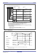
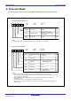
Figure 5.8 Low Voltage Detection Interrupt Generation Block
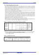
Figure 5.9 Low voltage Detection Interrupt Generation Circuit Operation Example
Low voltage detection interrupt generation circuit
Watchdog
timer interrupt
signal
D42 bit is set to 0 (not detected) by
writing a 0 in a program. VC27 bit is
set to 0 (low voltage
detection circuit
disabled), the D42 bit is set to 0.
VC27
VC13
Low voltage detection circuit
D4INT clock(the
clock with which it
operates also in
wait mode)
D42
DF1, DF0
1/2
00
2
01
2
10
2
11
2
1/21/21/8
Non-maskable
interrupt signal
Oscillation stop,
re-oscillation
detection
interrupt signal
Low voltage
detection
interrupt signal
Watchdog timer block
This bit is set to 0 (not detected) by writing a 0 by program.
Watchdog timer
underflow signal
D43
D41
CM02
WAIT instruction (wait mode)
D40
V
CC
Vref
+
-
Noise
rejection
(Rejection wide:200 ns)
Low voltage detection
signal
“H” when VC27 bit = 0
(disabled)
Noise rejection
circuit
Digital
filter
CM10
Output of the digital filter
(2)
D42 bit
L
o
w
v
o
l
t
a
g
e
d
e
t
e
c
t
i
o
n
i
n
t
e
r
r
u
p
t
s
i
g
n
a
l
N
o
l
o
w
v
o
l
t
a
g
e
d
e
t
e
c
t
i
o
n
i
n
t
e
r
r
u
p
t
s
i
g
n
a
l
s
a
r
e
g
e
n
e
r
a
t
e
d
w
h
e
n
t
h
e
D
4
2
b
i
t
i
s
1
.
s
a
m
p
l
i
n
g
S
e
t
t
o
0
b
y
p
r
o
g
r
a
m
(
n
o
t
d
e
t
e
c
t
e
d
)
VC13 bit
VC
C
sampling s
a
m
p
l
i
n
gs
a
m
p
l
i
n
g
S
e
t
t
o
0
b
y
a
p
r
o
g
r
a
m
(
n
o
t
d
e
t
e
c
t
e
d
)
NOTES:
1. D40 bit in the D4INT register is set to 1 (low voltage
detection interrupt enabled).
2. Output of the digital filter shown in Figure 5.8.