
Datasheet


20. Flash Memory Version
puorG92/C61M
page 341
854fo7002,03.raM21.1.veR
2110-1010B90JER
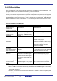
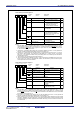
Figure 20.6 FMR0 and FMR1 Registers
NOTES:
Flash Memory Control Register 0
Symbol
Address
After Reset
FMR0 01B7
16
00000001
2
b7 b6 b5 b4 b3 b2 b1 b0
FMR00
Bit Symbol
Bit Name Function RW
0: Busy (during writing or erasing)
1: Ready
CPU rewrite mode select bit
(1)
0: Disables CPU rewrite mode
(Disables software command)
1: Enables CPU rewrite mode
(Enables software commands)
FMR01
Block 0, 1 rewrite enable bit
(2)
Set write protection for user ROM area
(see Table 20.4)
Flash memory stop bit
(3, 5)
FMR02
FMSTP
0
RY/BY status flag
Reserved bit
Set to 0
0: Successfully completed
1: Completion error
Program status flag
FMR06
0: Successfully completed
1: Completion error
Erase status flag
FMR07
RW
RW
RW
RW
RO
RO
RO
(b5-b4)
0: Starts flash memory operation
1: Stops flash memory operation
(Enters low-power consumption state
and flash memory reset)
0
(4)
(4
)
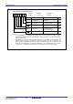
Flash Memory Control Register 1
Symbol
Address
After Reset
FMR1 01B5
16
000XXX0X
2
b7 b6 b5 b4 b3 b2 b1 b0
Bit Symbol
Bit Name Function
EW mode 1 select bit
(1)
0: EW mode 0
1: EW mode 1
FMR11
Block A, B access wait bit
(3)
Reserved bit When read, the content is undefined
Reserved bit
Set to 0
Nothing is assigned. If necessary, set to 0.
When read, the content is undefined
RW
RO
RW
RW
RW
(b0)
(b4)
Reserved bit
(b3-b2)
RO
NOTES:
(b5)
FMR16
RW
Block 0 to 5 rewrite enable
bit
(2)
FMR17
Set write protection for user ROM
space (see Table 20.4)
0: Disable
1: Enable
0: PM17 enabled
1: With wait state (1 wait)
When read, the content is undefined
0
1. Set the FMR11 bit to 1 immediately after setting it first to 0 while the FMR01 bit is set to 1. Do not
generate an interrupt or a DMA transfer between setting the bit to 0 and setting it to 1. Set this bit while
the P8
5/NMI/SD pin is held "H" when the NMI function is selected. If the FMR01 bit is set to 0, the FMR01
bit and FMR11 bit are both set to 0.
2. Set this bit to 1 immediately after setting it first to 0 while the FMR01 bit is set to 1. Do not generate an
interrupt or a DMA transfer between setting this bit to 0 and setting it to 1.
3. When rewriting more than 100 times, set this bit to 1 (with wait state). When the FMR17 bit is set to1(with
wait state), regardless of the PM17 bit setting, 1 wait state is inserted when accessing to blocks A and B.
The PM17 bit setting is enabled, regardless of the FMR17 bit setting, as to the access to other block and
the internal RAM.
1. Set the FMR01 bit to 1 immediately after setting it first to 0. Do not generate an interrupt or a DMA
transfer between setting the bit to 0 and setting it to 1. Set this bit while the P8
5/NMI/SD pin is held “H”
when selecting the NMI function. Set by program in a space other than the flash memory in EW mode
0. Set this bit to read alley mode and 0.
2. Set this bit to 1 immediately after setting it first to 0 while the FMR01 bit is set to 1. Do not generate an
interrupt or a DMA transfer between setting this bit to 0 and setting it to 1.
3. Set this bit in a space other than the flash memory by program. When this bit is set to 1, access to
flash memory will be denied. To set this bit to 0 after setting it to 1, wait for 10 usec. or more after
setting it to 1. To read data from flash memory after setting this bit to 0, maintain tps wait time before
accessing flash memory.
4. This bit is set to 0 by executing the clear status command.
5. This bit is enabled when the FMR01 bit is set to 1 (CPU rewrite mode). If the FMR01 bit is set to 0, this
bit can be set to 1 by writing 1 to the FMR01 bit. However, the flash memory does not enter low-power
consumption status and it is not initialized.