
Datasheet


15. A/D Converter
puorG92/C61M
page 251
854fo7002,03.raM21.1.veR
2110-1010B90JER
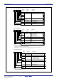
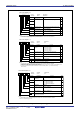
Figure 15.27 ADCON0 to ADCON2 Registers in Delayed Trigger Mode 1
A/D Control Register 0
(1)
Symbol Address After Reset
ADCON0 03D6
16
00000XXX
2
b7 b6 b5 b4 b3 b2 b1 b0
Analog input pin
select bit
CH0
Bit Symbol Bit Name Function
CH1
CH2
A/D operation mode
select bit 0
MD0
MD1
Trigger select bit Refer to Table 15.13
TRG
ADST
A/D conversion start flag
(2)
0 : A/D conversion disabled
1 : A/D conversion started
Frequency select bit 0CKS0
RW
A/D Control Register 1
(1)
Symbol Address After Reset
ADCON1 03D7
16
00
16
Bit Name FunctionBit Symbol
b7 b6 b5 b4 b3 b2 b1 b0
A/D sweep pin
select bit
(2)
SCAN0
SCAN1
MD2
BITS
8/10-bit mode select bit 0: 8-bit mode
1: 10-bit mode
VCUT
Vref connect bit
(3)
A/D operation mode
select bit 1
1: Vref connected
01
When selecting delayed trigger mode 1
0
1 1 1: Set to 111b in delayed trigger
mode 1
b2 b1 b0
0 0 : One-shot mode or delayed trigger mode
0,1
b4 b3
1
Frequency select bit 1
CKS1
0: Any mode other than repeat sweep
mode 1
RW
RW
RW
RW
RW
RW
RW
RW
RW
RW
RW
RW
RW
RW
RW
Refer to Table 15.2
NOTES:
1. If the ADCON0 register is rewritten during A/D conversion, the conversion result will be undefined.
2. Do not write 1 in delayed trigger mode 1. If necessary, set to 0.
NOTES:
1. If the ADCON1 register is rewritten during A/D conversion, the conversion result will be undefined.
2. AN0
0
to AN0
7
, AN2
0
to AN2
7
, and AN3
0
to AN3
2
can be used in the same way as AN
0
to AN
7
. Use bits ADGSEL1 and
ADGSET0 in the ADCON2 register to select the desired pin.
3. If the VCUT bit is reset from 0 (Vref unconnected) to 1 (Vref connected), wait for 1 µs or more before starting
A/D conversion.
Refer to Table 15.2
(b7-b6)
110
b1 b0
0 0: AN
0
to AN
1
(2 pins)
0 1: AN
0
to AN
3
(4 pins)
1 0: AN
0
to AN
5
(6 pins)
1 1: AN
0
to AN
7
(8 pins)
0
Nothing is assigned. If necessary, set to 0.
When read,
the
content is undefined
NOTES:
1. If the ADCON2 register is rewritten during A/D conversion, the conversion result will be undefined.
2. Set to 1 in delayed trigger mode 1.
A/D Control Register 2
(1)
Symbol Address After Reset
ADCON2 03D4
16
00
16
b7 b6 b5 b4 b3 b2 b1 b0
A/D conversion method
select bit (2)
1: With sample and hold
Bit Symbol Bit Name Function RW
SMP
Reserved bit
Set to
0
0
A/D input group
select bit
0 0: Select port P10 group
0 1: Select port P9 group
1 0: Select port P0 group
1 1: Select port P1/P9 group
b2 b1
Frequency select bit 2
CKS2
ADGSEL0
ADGSEL1
RW
RW
RW
RW
RW
(b3)
Nothing is assigned. If necessary, set to 0.
When read, the content is 0
(b7-b6)
Refer to Table 15.2
RW
TRG1
Trigger select bit 1
1
Refer to Table 15.13
1