
Datasheet

15. A/D Converter
puorG92/C61M
page 224
854fo7002,03.raM21.1.veR
2110-1010B90JER
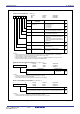
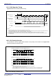
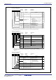
Figure 15.2 ADCON0 to ADCON2 Registers
A/D Control Register 0
(1)
Symbol Address After Reset
ADCON0 03D6
16
00000XXX
2
b7 b6 b5 b4 b3 b2 b1 b0
Analog input pin select bit
CH0
Bit Symbol Bit Name Function
CH1
CH2
A/D operation mode
select bit 0
MD0
MD1
Trigger select bit
0: Software trigger
1: Hardware trigger
TRG
ADST
A/D conversion start flag
0: A/D conversion disabled
1: A/D conversion started
Frequency select bit 0
See Table 15.2
CKS0
RW
NOTE:
1. If the ADCON0 register is rewritten during A/D conversion, the conversion result will be undefined.
RW
RW
RW
RW
RW
RW
RW
RW
Function varies with each operation mode
b4 b3
0 0: One-shot mode or Delayed trigger
mode 0,1
0 1: Repeat mode
1 0: Single sweep mode or Simultaneous
sample sweep mode
1 1: Repeat sweep mode 0 or Repeat
sweep mode 1
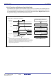
A/D Control Register 1
(1)
Symbol Address After Reset
ADCON1 03D7
16
00
16
Bit Name Function
Bit Symbol
b7 b6 b5 b4 b3 b2 b1 b0
A/D sweep pin select bit
SCAN0
SCAN1
MD2
BITS 8/10-bit mode select bit
0 : 8-bit mode
1 : 10-bit mode
VCUT
A/D operation mode
select bit 1
0 : Other than repeat sweep mode 1
1 : Repeat sweep mode 1
0 : Vref not connected
1 : Vref connected
Frequency select bit 1CKS1
RW
RW
RW
RW
RW
RW
RW
Function varies with each operation mode
See Table 15.2
Nothing is assigned. If necessary, set to 0.
When read, its content is 0
(b7-b6)
NOTES:
1. If the ADCON1 register is rewritten during A/D conversion, the conversion result will be undefined.
2. If the VCUT bit is reset from 0 (V
REF
unconnected) to 1 (V
REF
connected), wait for 1 µs or more before starting A/D
conversion.
Vref connect Bit
(2)
0
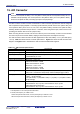
A/D Control Register 2
(1)
Symbol Address After Reset
ADCON2 03D4
16
00
16
Bit Name FunctionBit Symbol
b7 b6 b5 b4 b3 b2 b1 b0
A/D conversion method
select bit
SMP
Reserved bit Set to 0
TRG1
A/D input group select bit
b2 b1
0 0: Select port P10 group
0 1: Select port P9 group
1 0: Select port P0 group
1 1: Select port P1/P9 group
Function varies with each operation mode
Frequency select bit 2CKS2
RW
RW
RW
RW
RW
RW
RW
0: Without sample and hold
1: With sample and hold
See Table 15.2
Nothing is assigned. If necessary, set to 0.
When read, the content is 0
(b7-b6)
NOTS:
1. If the ADCON2 register is rewritten during A/D conversion, the conversion result will be undefined.
Trigger select bit
ADGSEL0
ADGSEL1
(b3)