
Datasheet

14. Serial I/O
puorG92/C61M
page 200
854fo7002,03.raM21.1.veR
2110-1010B90JER
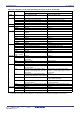
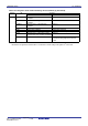
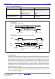
Table 14.13 I
2
C bus mode Functions
Function
I
2
C bus mode (SMD2 to SMD0 = 0102, IICM = 1)
Clock synchronous serial I/O
mode (SMD2 to SMD0 = 001
2
,
IICM = 0)
Factor of interrupt number
15
(1)
(Refer to Fig.14.23)
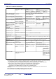
No acknowledgment
detection (NACK)
Rising edge of SCL
2 9th bit
Factor of interrupt number
16
(1)
(Refer to Fig.14.23)
Start condition detection or stop condition detection
(Refer to Table 14.14)
UART2 transmission
output delay
Functions of P7
0 pin
Noise filter width
Read RxD2 and SCL
2 pin
levels
Factor of interrupt number
10
(1)
(Refer to Fig.14.23)
Acknowledgment detection
(ACK)
Rising edge of SCL
2 9th bit
Initial value of TxD2 and
SDA
2 outputs
UART2 transmission
Transmission started or
completed (selected by U2IRS)
UART2 reception
When 8th bit received
CKPOL = 0 (rising edge)
CKPOL = 1 (falling edge)
Not delayed
TxD2 output
RxD2 input
CLK2 input or output selected
15ns
Possible when the
corresponding port direction bit
= 0
CKPOL = 0 (H)
CKPOL = 1 (L)
Delayed
SDA
2 input/output
SCL
2 input/output
(Cannot be used in I
2
C bus mode)
Initial and end values of
SCL
2
H
200ns
Always possible no matter how the corresponding port direction bit is set
The value set in the port register before setting I
2
C bus mode
(2)
Timing for transferring data
from the UART reception
shift register to the U2RB
registe
r
IICM2 = 0
(NACK/ACK interrupt)
IICM2 = 1
(UART transmit/ receive interrupt)
CKPH = 1
(Clock delay)
CKPH = 1
(Clock delay)
UART2 transmission
Rising edge of
SCL
2 9th bit
UART2 transmission
Falling edge of SCL
2
next to the 9th bit
UART2 transmission
Falling edge of SCL
2 9th bit
CKPOL = 0 (rising edge)
CKPOL = 1 (falling edge)
Rising edge of SCL
2 9th bit
Falling edge of
SCL
2 9th bit
Falling and rising
edges of SCL
2 9th
bit
.
.
DMA1 factor (Refer to Fig.
14.23)
UART2 reception
Acknowledgment detection
(ACK)
UART2 reception
Falling edge of SCL
2
9th bi
t
Store received data
1st to 8th bits are stored in
bits bit 7 to 0 in the U2RB
register
1st to 8th bits are stored in
bits bit 7 to 0 in the U2RB
register
1st to 7th bits are stored into the bit 6 to
bit 0 in the U2RB register, with 8th bit
stored in the bit 8 in the U2RB register
L
Read U2RB register
Bit 6 to bit 0 as bit 7
to bit 1, and bit 8 as
bit 0
(4)
Read received data
U2RB register status is read
directly as is
CKPH = 0
(No clock delay)
CKPH = 0
(No clock delay)
HL
1st to 8th bits are
stored in U2RB
register bit 7 to bit 0
(3)
Functions of P71 pin
Functions of P7
2 pin
NOTES:
1. If the source or cause of any interrupt is changed, the IR bit in the interrupt control register for the changed interrupt
may inadvertently be set to 1 (interrupt requested). (Refer to “Notes on interrupts” in Precautions.)
If one of the bits shown below is changed, the interrupt source, the interrupt timing, etc. change. Therefore,
always be sure to clear the IR bit to 0 (interrupt not requested) after changing those bits
Bits SMD2 to the SMD0 in the U2MR register, the IICM bit in the U2SMR register,
the IICM2 bit in the U2SMR2 register, the CKPH bit in the U2SMR3 register
2. Set the initial value of SDA
2
output while bits SMD2 to SMD0 in the U2MR register is set to 000
2
(serial I/O
disabled).
3. Second data transfer to U2RB register (Rising edge of SCL
2
9th bit)
4. First data transfer to U2RB register (Falling edge of SCL
2
9th bit)