
Datasheet

14. Serial I/O
puorG92/C61M
page 197
854fo7002,03.raM21.1.veR
2110-1010B90JER
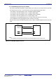
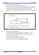
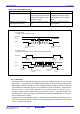
Figure 14.22 I
2
C bus mode Block Diagram
CLK
control
Falling edge
detection
External
clock
Internal clock
Start/stop condition
detection interrupt
request
Start condition
detection
Stop condition
detection
Reception register
Bus
busy
Transmission
register
Arbitration
Noise
Filter
SDA2
SCL2
UART2
D
T
Q
D
T
Q
D
T
Q
NACK
AC
K
UART2
UART2
UART2
R
UART2 transmit,
NACK interrupt
request
UART2 receive,
ACK interrupt request,
DMA1 request
IICM=1 and
IICM2=0
S
R
Q
ALS
R
S
SWC
IICM=1 and
IICM2=0
IICM2=1
IICM2=1
SWC2
SDHI
DMA0, DMA1 request
Noise
Filter
IICM=0
IICM=1
DMA0
STSPSEL=0
STSPSEL=1
STSPSEL=1
STSPSEL=0
SDA
STSP
SCL
STSP
ACKC=1 ACKC=0
Q
Port register
(1)
I/O port
9th bit falling edge
9th bit
ACKD bit
Delay
circuit
Start and stop condition generation block
This diagram applies to the case where bits SMD2 to SMD0 in the U2MR register is set to 010
2
and the IICM bit in the U2SMR register
is set to 1.
IICM : Bit in the U2SMR register
IICM2, SWC, ALS, SWC2, SDHI : Bits in the U2SMR2 register
STSPSEL, ACKD, ACKC : Bits in the U2SMR4 register
NOTE:
1. If the IICM bit is set to 1, the pin can be read even when the PD7_1 bit is set to 1 (output mode).