
Datasheet


14.Serial I/O
puorG92/C61M
page 174
854fo7002,03.raM21.1.veR
2110-1010B90JER
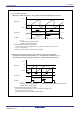
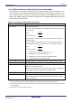
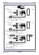
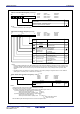
Figure 14.4 U0TB to U2TB, U0RB to U2RB, U0BRG to U2BRG Registers
(b15)
b7 b0
(b8)
b7
b0
UARTi Transmit Buffer Register (i=0 to 2)
(1)
Function
Transmit data
Nothing is assigned. If necessary, set to 0.
When read, their contents are undefined
Symbol Address After Reset
U0TB 03A3
16-03A216 Undefined
U1TB 03AB
16-03AA16 Undefined
U2TB 037B
16-037A16 Undefined
NOTES:
1. Use MOV instruction to write to this register.
RW
WO
b7
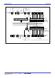
UARTi Baud Rate Generation Register (i=0 to 2)
(1, 2, 3)
b0
Symbol Address After Reset
U0BRG 03A1
16 Undefined
U1BRG 03A9
16 Undefined
U2BRG 0379
16 Undefined
Function
Assuming that set value = n, UiBRG divides
the count source by n + 1
Setting Range
NOTES:
1. Write to this register while serial I/O is neither transmitting nor receiving.
2. Use MOV instruction to write to this register.
The transfer clock is shown below when the setting value in the UiBRG register is set as n.
(1) When the CKDIR bit in the UiMR register to 0 (internal clock)
• Clock synchronous serial I/O mode : fj/(2(n+1))
• Clock asynchronous serial I/O (UART) mode : fj/(16(n+1))
(2) When the CKDIR bit in the UiMR register to 1 (external clock)
• Clock synchronous serial I/O mode : f
EXT
• Clock asynchronous serial I/O (UART) mode : fEXT/(16(n+1))
fj : f1SIO, f2SIO, f8SIO, f32SIO
f
EXT : Input from CLKi pin
3. Set the UiBRG register after setting bits CLK1 and CLK0 in the registers UiC0.
RW
WO
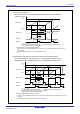
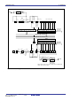
(b15)
Symbol Address After Reset
U0RB 03A7
16-03A616 undefined
U1RB 03AF
16-03AE16 undefined
U2RB 037F
16-037E16 undefined
b7 b0
(b8)
b7 b0
UARTi Receive Buffer Register (i=0 to 2)
Function
Bit Name
Bit
Symbol
0 : No framing error
1 : Framing error found
0 : No parity error
1 : Parity error found
0 : No error
1 : Error found
OER
FER
PER
SUM
Overrun error flag
(1)
Framing error flag
(1)
Parity error flag
(1)
Error sum flag
(1)
0 : No overrun error
1 : Overrun error found
ABT
Arbitration lost
detecting flag
(2)
0 : Not detected
1 : Detected
(b7-b0)
(b10-b9)
(b8)
Nothing is assigned. If necessary, set to 0.
When read, their contents are undefined
RW
RO
RW
RO
RO
RO
RO
RO
0016 to FF16
Receive data (D8)
Receive data (D7 to D0)
NOTES:
1. When the SMD2 to SMD0 bits in the UiMR register are set to 000
2 (serial I/O disabled) or the RE bit in the UiC1 register is set to
0 (reception disabled), all bits SUM, PER, FER and OER are set to 0 (no error). The SUM bit is set to 0 (no error) when all of the
PER, FER and OER bits are set to 0 (no error). Also, bits PER and FER are set to 0 by reading the lower byte of the UiRB
register.
2. The ABT bit is set to 0 by setting to 0 by program. (Writing 1 has no effect.) Nothing is assigned at the bit 11 in the U0RB and
U1RB registers. If necessary, set to 0. When read, its content is 0.