
Datasheet


14. Serial I/O
puorG92/C61M
page 173
854fo7002,03.raM21.1.veR
2110-1010B90JER
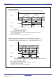
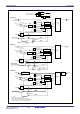
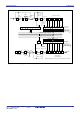
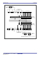
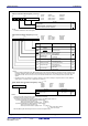
Figure 14.3 Block diagram of UART2 transmit/receive unit
SP SP
PAR
2SP
1SP
UART
UART
(7 bits)
UART
(8 bits)
UART(7 bits)
UART
(9 bits)
Clock
synchronous
type
Clock
synchronous type
Data bus low-order bits
TxD2
UARTi transmit register
PAR
disabled
PAR
enabled
D8
D7 D6 D5 D4 D3 D2 D1 D0
UART2 transmit
buffer register
UART
(8 bits)
UART
(9 bits)
Clock
synchronous type
UART2 receive
buffer registe
r
UARTi receive register
2SP
1SP
UART
(7 bits)
UART
(8 bits)
UART(7 bits)
UART
(9 bits)
Clock
synchronous type
Clock
synchronous type
RxD2
UART
(8 bits)
UART
(9 bits)
Address 037E
16
Address 037F16
Address 037A16
Address 037B16
Data bus high-order bits
D7 D6 D5 D4 D3 D2 D1 D0D8
0000000
SP SP
PAR
0
Reverse
No revers
e
Error signal
output circui
t
RxD data
reverse circuit
Error signal output
enable
Error signal output
disable
Reverse
No reverse
Logic reverse circuit + MSB/LSB conversion circuit
Logic reverse circuit + MSB/LSB conversion circuit
PAR
enabled
PAR
disabled
UART
Clock
synchronous
type
TxD data
reverse circuit
SP: Stop bit
PAR: Parity bit
STPS=0
STPS=1
PRYE=0
PRYE=1
STPS=0
STPS=1
PRYE=0
PRYE=1
IOPOL=0
IOPOL=1
IOPOL
=0
IOPOL
=1
U2ERE
=0
U2ERE
=1
SMD2 to SMD0, STPS, PRYE, IOPOL, CKDIR : Bits in the U2MR register
U2ERE : Bits in the U2C1 register