
Datasheet


14. Serial I/O
puorG92/C61M
page 171
854fo7002,03.raM21.1.veR
2110-1010B90JER
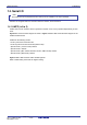
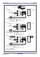
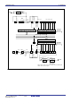
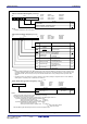
Figure 14.1 Block diagram of UARTi (i = 0 to 2)
Clock synchronous type
(when internal clock is selected)
Clock synchronous type
(when external clock is selected)
Clock source selection
Internal
External
CTS/RTS disabled
CTS/RTS selected
RxD
0
1 / (n0+1)
1/16
1/16
1/2
U0BRG
registe
r
CLK
0
CTS
0
/ RTS
0
f
1SIO or
f
2SIO
f
8SIO
f
32SIO
V
CC
RTS
0
CTS
0
TxD
0
(UART0)
CLK1 to CLK0
00
2
01
2
10
2
CKDIR=0
CKDIR=1
CKPOL
CKDIR=0
CKDIR=
1
CRS=1
CRS=0
CRD=0
CRD=1
RCSP=0
RCSP=1
V
CC
CRD=0
CRD=1
UART reception
Clock synchronous
type
UART transmission
Clock synchronous
type
Clock synchronous type
(when internal clock is selected)
Receive
clock
Transmit
clock
Reception
control circuit
Transmission control
circuit
Transmit/
receive
unit
CLK
polarity
reversing
circuit
CTS/RTS disabled
CTS
0
from UART1
UART reception
Clock synchronous
type
RxD
1
TxD
1
(UART1)
1 / (n1+1)
1/16
1/16
1/2
U1BRG
register
CLK
1
f
1SIO or
f
2SIO
f
8SIO
f
32SIO
CLK1 to CLK0
00
2
01
2
10
2
CKDIR=0
CKDIR=1
CKPOL
CKDIR=0
CKDIR=
1
V
CC
CRD=0
CRD=1
CLKMD0=0
CLKMD1=0
CRS=1
CRS=0
RCSP=0
RCSP=1
CLKMD0=1
CLKMD1=1
Clock source selection
Internal
External
UART transmission
Clock synchronous
type
Clock synchronous type
(when internal clock is selected)
Receive
clock
Transmit
clock
Reception
control circuit
Transmission
control circuit
Transmit/
receive
unit
Clock synchronous type
(when external clock is selected)
Clock synchronous type
(when internal clock is selected)
CLK
polarity
reversing
circuit
RTS1
CTS1
Clock output
pin select
CTS/RTS disable
d
CTS/RTS disable
d
CTS/RTS selecte
d
CTS
0
from UART0
CTS
1
/ RTS
1
/
CTS
0
/ CLKS
1
i = 0 to 2
n
i
: Values set to the UiBRG register
SMD2 to SMD0, CKDIR: Bists in the UiMR register
CLK1 to CLK0, CKPOL, CRD, CRS: Bits in the UiC0 register
CLKMD0, CLKMD1, RCSP: Bits in the UCON register
RxD
2
CLK
2
CTS
2
/ RTS
2
RTS
2
CTS
2
TxD
2
(UART2)
1 / (n2+1)
1/16
1/16
1/2
U2BRG
registe
r
f
1SIO or
f
2SIO
f
8SIO
f
32SIO
CLK1 to CLK0
00
2
01
2
10
2
CKDIR=0
CKDIR=1
CKPOL
CKDIR=0
CKDIR=
1
CRS=1
CRS=0
V
CC
CRD=0
CRD=1
Reception
control circuit
Transmission
control circuit
UART reception
Clock synchronous
type
UART transmission
Clock synchronous
type
Clock synchronous type
(when internal clock is selected)
Receive
clock
Transmit
clock
RxD polarity
reversing circuit
Internal
External
Clock source selection
TxD
polarity
reversing
circuit
Transmit/
receive
unit
Clock synchronous type
(when internal clock is selected)
Clock synchronous type
(when external clock is selected)
CLK
polarity
reversing
circuit
CTS/RTS disabled
CTS/RTS disabled
CTS/RTS
selecte
d
Main clock, PLL clock,
or on-chip oscillator clock
1/2
1/8
1/4
f
1SIO
f
2SIO
f
8SIO
f
32SIO
f
1SIO or
f
2SIO
PCLK1=1
PCLK1=0