
Datasheet


13. Timer S
puorG92/C61M
page 159
854fo7002,03.raM21.1.veR
2110-1010B90JER
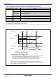
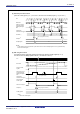
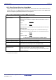
Figure 13.20 Time Measurement Function (2)
2. No interrupt is generated if the MCU receives a trigger signal when the G1IRj bit is set to 1.
1. Bits in the G1IR register.
2. Input pulse applied to the INPC1j pin requires 1.5 f
BT1
clock cycles or more.
n-2 n-1
n
n+1 n+2 n+3 n+4 n+5 n+6 n+7 n+8 n+9 n+10 n+11 n+12 n+13 n+14
n n +5 n+8
n-2 n-1 n n+1 n+2 n+3 n+4 n+5 n+6 n+7 n+8 n+9 n+10 n+11 n+12 n+13 n+14
n n+2 n+5 n+8
n+12
Delayed by 1 clock
f
BT1
Base timer
INPC1j pin input or
trigger signal after
passing the digital
filter
G1TMj register
(a)
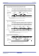
When selecting the rising edge as a timer measurement trigger
(Bits CTS1 and CTS0 in the G1TMCRj register (j=0 to 7)=01
2
)
G1IRj bit
(1)
write 0 by program if setting to 0
NOTES :
.
(2)
(b) When selecting both edges as a timer measurement trigger
(Bits CTS1 and CTS0 = 11
2
)
Maximum 3.5 f
1
or f
2
or f
BT1
clock cycles
(1)
(c) Trigger signal when using digital filter
(Bits DF1 to DF0 in the G1TMCRj register =10
2
or 11
2
)
Signals, which do not match 3
times, are stripped off
f
BT1
Base timer
INPC1j pin input or
trigger signal after
passing the digital
filter
G1TMj register
(2)
G1IRj bit
(1)
f
1
or f
2
or f
BT1
(1)
INPC1j pin
Trigger signal after
passing the digital
filter
NOTES :
.
1. Bits in the G1IR register.
However, the value of the G1TMj register is updated.
NOTE:
1. f
BT1
when bits DF1 to DF0 are set to 102, and f
1
or f
2
when set to 112.
The trigger signal is delayed
by the digital filter
write 0 by program
if setting to 0