
Datasheet


13. Timer S
puorG92/C61M
page 148
854fo7002,03.raM21.1.veR
2110-1010B90JER
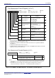
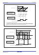
Figure 13.8 G1FS and G1FE Registers
Function Enable Register
(1)
Symbol Address After Reset
G1FE
0326
16
00
16
b7 b6 b5 b4 b3 b2 b1 b0
RW
RW
RW
RW
RW
RW
RW
RW
RW
Bit Name
Bit
Symbol
IFE0
IFE1
IFE2
Channel 0 function enable bit
IFE3
IFE4
IFE5
IFE7
Function
IFE6
0 : Disable function s for channel j
(2)
1 : Enable functions for channel j
(j=0 to 7)
Channel 1 function enable bit
Channel 2 function enable bit
Channel 3 function enable bit
Channel 4 function enable bit
Channel 5 function enable bit
Channel 6 function enable bit
Channel 7 function enable bit
NOTES:
1.
The G1FE register reflects the base timer value, synchronizing with the count source f
BT1
cycles.
2.
When functions for the channel j are disabled, each pin functions as an I/O port.
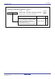
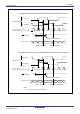
Function Select Register
Symbol Address After Reset
G1FS
0327
16
00
16
b7 b6 b5 b4 b3 b2 b1 b0
RW
RW
RW
RW
RW
RW
RW
RW
RW
Bit Name
Bit
Symbol
FSC0
FSC1
FSC2
Channel 0 time measure-
ment/waveform generating
function select bit
FSC3
FSC4
FSC5
FSC7
Function
FSC6
0: Select the waveform generating
function
1: Select the time measurement
function
Channel 1 Time Measure-
ment/Waveform Generating
Function Select Bit
Channel 2 time measure-
ment/waveform generating
function select bit
Channel 3 time measure-
ment/waveform generating
function select bit
Channel 4 time measure-
ment/waveform generating
function select bit
Channel 5 time measure-
ment/waveform generating
function select bit
Channel 6 time measure-
ment/waveform generating
function select bit
Channel 7 time measure-
ment/waveform generating
function select bit