
Datasheet


13. Timer S
puorG92/C61M
page 146
854fo7002,03.raM21.1.veR
2110-1010B90JER
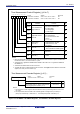
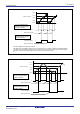
Figure 13.6 G1TM0 to G1TM7 Registers, and G1POCR0 to G1POCR7 Registers
Waveform Generation Control Register j (j=0 to 7)
Symbol Address After Reset
G1POCR0 to G1POCR3 0310
16
, 0311
16
, 0312
16
, 0313
16
0X00 XX00
2
G1POCR4 to G1POCR7 0314
16
, 0315
16
, 0316
16
, 0317
16
0X00 XX00
2
RW
RW
RW
RW
RW
RW
Bit Name Function
Bit
Symbol
MOD0
MOD1
Operating mode
select bit
Output initial value
select bit
(4)
IVL
RLD
INV
0: "L" output as a default value
1: "H" output as a default value
Inverse output function
select bit
(2)
: Single waveform output mode
: SR waveform output mode
(1)
: Phase-delayed waveform
output mode
: Do not set to this value
0: Output is not inversed
1: Output is inversed
b1
0
0
1
1
b0
0
1
0
1
G1POj register value
reload timing select bit
NOTES :
1. This setting is enabled only for even channels. In SR waveform output mode, values written to the
corresponding odd channel (next channel after an even channel) are ignored. Even channels
provide waveform output. Odd channels provide no waveform output.
2. The inverse output function is the final step in waveform generating process. When the INV bit is set
to 1, and "H" signal is provided a default output by setting the IVL bit to 0, and an "L" signal is
provided by setting it to 1.
3. In the SR waveform output mode, set not only the even channel but also the correspoinding even
channel (next channel after the even channel).
4. To provide either "H" or "L" signal output set in the IVL bit, set the FSCj bit in the G1FS register to 0
(select waveform generating function) and IFEj bit in the G1FE register to 1 (functions for channel j
enabled). Then set the IVL bit to 0 or 1.
Nothing is assigned. If necessary, set to 0.
When read, their contents are undefined
Nothing is assigned. If necessary, set to 0.
When read, its content is undefined
0: Reloads the G1POj register when
value is written
1: Reloads the G1POj register when
the base timer is reset
(b3-b2)
(b6)
b7 b6 b5 b4 b3 b2 b1 b0
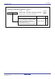
Waveform Generation Register j (j=0 to 7)
Symbol
G1TM0 to G1TM2
G1TM3 to G1TM5
G1TM6 to G1TM7
RW
RO
Function Setting Range
b15
(b7)
b8
(b0)
Address
030116-030016, 030316-030216, 030516-030416
030716-030616, 030916-030816, 030B16-030A16
030D16-030C16, 030F16-030E16
After Reset
Indeterminte
Indeterminte
Indeterminte
The base timer value is stored every
measurement timing
b7 b0