
Datasheet


12. Timer A
puorG92/C61M
page 116
854fo7002,03.raM21.1.veR
2110-1010B90JER
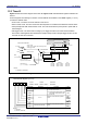
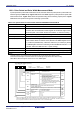
Figure 12.13 Example of 16-bit Pulse Width Modulator Operation
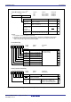
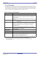
Figure 12.14 Example of 8-bit Pulse Width Modulator Operation
1 / f
i
X (2 – 1)
16
Count source
Input signal to
TA
iIN pin
PWM pulse output
from TA
iOUT pin
Trigger is not generated by this signal
“H”
“H”
“L”
“L”
IR bit in the
TAiIC register
1
0
fj : Frequency of count source
(f
1, f2, f8, f32, fC32)
i = 0 to 4
NOTES:
1. n = 0000
16 to FFFE16.
2. This timing diagram is for the case where the TAi register is 0003
16, bits TAiTGH and TAiTGL in the ONSF or
TRGSR register is set to 00
2 (TAiIN pin input), the MR1 bit in the TAiMR register is set to 1 (rising edge), and
the MR2 bit in the TAiMR register is set to 1 (trigger selected by TAiTGH and TAiTGL bits).
1 / f
j
X
n
Set to 0 upon accepting an interrupt request or by program
Count source
(1)
Input signal to
TA
iIN pin
Underflow signal of
8-bit prescaler
(2)
PWM pulse output
from TA
iOUT pin
“H”
“H”
“H”
“L”
“L”
“L”
1
0
Set to 0 upon accepting an interrupt request or by program
1 / f
j
X (m
+ 1) X (2 – 1)
8
1 / fj X (m + 1) X n
1 / fj X (m + 1)
IR bit in the
TAiIC register
f
j : Frequency of count source
(f
1, f2, f8, f32, fC32)
i = 0 to 4
NOTES:
1. The 8-bit prescaler counts the count source.
2. The 8-bit pulse width modulator counts the 8-bit prescaler's underflow signal.
3. m = 00
16 to FF16; n = 0016 to FE16.
4. This timing diagram is for the case where the TAi register is 0202
16, bits TAiTGH and TAiTGL in the ONSF or
TRGSR register is set to 00
2 (TAiIN pin input), the MR1 bit in the TAiMR register is set to 0 (falling edge), and the
MR2 bit in the TAiMR register is set to 1 (trigger selected by bits TAiTGH and TAiTGL).