
Datasheet

12. Timer A
puorG92/C61M
page 113
854fo7002,03.raM21.1.veR
2110-1010B90JER
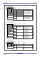
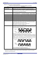
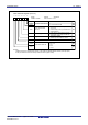
Figure 12.11 TAiMR Register in One-shot Timer Mode
Bit Name
Timer Ai Mode Register (i=0 to 4)
Symbol
Address
After Reset
TA0MR to TA4MR 396
16
to 039A
16
00
16
Function
Bit Symbol
b7 b6 b5 b4 b3 b2 b1 b0
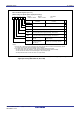
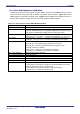
Operation mode select bit
1 0: One-shot timer mode
b1 b0
TMOD1
TMOD0
MR0
MR2
MR1
MR3 Set to 0 in one-shot timer mode
TCK1
TCK0
Count source select bit
100
Trigger select bit
External trigger select bit
(1)
RW
RW
RW
RW
RW
RW
RW
RW
RW
NOTES:
1. Effective when
bits TAiTGH and TAiTGL in the ONSF or TRGSR register are 002 (TAiIN pin input).
2. The port direction bit for the TAi
IN pin must be set to 0 (input mode).
0: Pulse is not output (TA
iOUT
pin functions
as I/O port)
1: Pulse is output (TAi
OUT
pin functions as a
pulse output pin)
0: TAiOS bit is enabled
1: Selected by bits TAiTGH to TAiTGL
0: Falling edge of input signal to TAiIN pin
(2)
1: Rising edge of input signal to TAiIN pin
(2)
Pulse output function
select bit
b7 b6
0 0: f
1
or f
2
0 1: f
8
1 0: f
32
1 1: f
C32