
Datasheet

12. Timer A
puorG92/C61M
page 110
854fo7002,03.raM21.1.veR
2110-1010B90JER
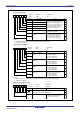
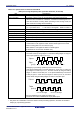
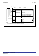
Figure 12.9 TA2MR to TA4MR Registers in Event Counter Mode (when using two-phase pulse
signal processing with timer A2, A3 or A4)
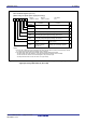
Timer Ai Mode Register (i=2 to 4)
(When using two-phase pulse signal processing)
Symbol Address After Reset
TA2MR to TA4MR 0398
16
to 039A
16
00
16
b6 b5 b4 b3 b2 b1 b0
Operation mode select bit
0 1: Event counter mode
b1 b0
TMOD1
TMOD0
MR0 To use two-phase pulse signal processing, set this bit to
0
MR2
MR1
MR3
TCK1
TCK0
010
Bit Name Functio
n
RW
Count operation type
select bit
Two-phase pulse signal
processing operation
select bit
(1)(2)
0: Reload type
1: Free-run type
0: Normal processing operation
1: Multiply-by-4 processing operation
001
To use two-phase pulse signal processing, set this bit to 0
To use two-phase pulse signal processing, set this bit to
1
To use two-phase pulse signal processing, set this bit to 0
Bit Symbol
RW
RW
RW
RW
RW
RW
RW
RW
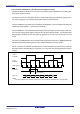
NOTES:
1. The TCK1 bit is valid for timer A3 mode register. No matter how this bit is set, timers A2 and A4 always operate
in normal processing mode and x4 processing mode, respectively.
2. If two-phase pulse signal processing is desired, following register settings are required:
• Set the TAiP bit in the UDF register to 1 (two-phase pulse signal processing function enabled).
• Set bits TAiTGH and TAiTGL in the TRGSR register to 00
2
(TAiIN pin input).
• Set the port direction bits for TAi
IN
and TAi
OUT
to 0 (input mode).