
Datasheet


12. Timer A
puorG92/C61M
page 104
854fo7002,03.raM21.1.veR
2110-1010B90JER
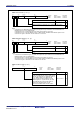
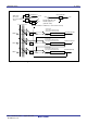
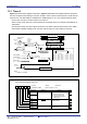
Figure 12.5 TA0 to TA4 Registers, TABSR Register, and UDF Register
Symbol Address After Reset
TA0 0387
16
, 0386
16
Undefined
TA1 0389
16
, 0388
16
Undefined
TA2 038B
16
, 038A
16
Undefined
TA3 038D
16
, 038C
16
Undefined
TA4 038F
16
, 038E
16
Undefined
b7 b0 b7 b0
(b15)
(b8)
Timer Ai Register (i= 0 to 4)
(1)
Function Setting Range
Timer
mode
Event
counter
mode
One-shot
timer mode
Mode RW
WO
RW
RW
WO
WO
Symbol Address After Reset
TABSR 0380
16
00
16
Count Start Flag
b7 b6 b5 b4 b3 b2 b1 b0
NOTES:
1. The register must be accessed in 16 bit units.
2. If the TAi register is set to 0000
16
, the counter does not work and timer Ai interrupt requests are not
generated either. Furthermore, if “pulse output” is selected, no pulses are output from the TAiOUT pin.
3. If the TAi register is set to 0000
16
, the pulse width modulator does not work, the output level on the
TAiOUT pin remains low, and timer Ai interrupt requests are not generated either. The same applies
when the 8 high-order bits of the timer TAi register are set to 0000
16
while operating as an 8-bit pulse
width modulator.
4. Use the MOV instruction to write to the TAi register.
5. The timer counts pulses from an external device or overflows or underflows in other timers.
Divide the count source by n + 1 where n = set
value
0000
16
to FFFE
16
(3, 4)
0000
16
to FFFF
16
0000
16
to FFFF
16
0000
16
to FFFF
16
(2, 4)
00
16
to FE
16
(High-order address)
00
16
to FF
16
(Low-order address)
(3, 4)
Modify the pulse width as follows:
PWM period: (2
8
– 1) x (m + 1)/ fj
High level PWM pulse width: (m + 1)n / fj where
n = high-order address set value, m = low-order
address set value, fj = count source frequency
Modify the pulse width as follows:
PWM period: (2
16
– 1) / fj
High level PWM pulse width: n / fj where n = set
value, fj = count source frequency
Divide the count source by n where n = set
value and cause the timer to stop
Divide the count source by FFFF
16
– n + 1
where n = set value when counting up or by n +
1 when counting down
(5)
Pulse width
modulation
mode
(16-bit PWM)
Pulse width
modulation
mode
(8-bit PWM)
Bit Name FunctionBit Symbol
0 : Stops counting
1 : Starts counting
Timer B2 count start flagTB2S
Timer B1 count start flagTB1S
Timer B0 count start flagTB0S
Timer A4 count start flagTA4S
Timer A3 count start flagTA3S
Timer A2 count start flagTA2S
Timer A1 count start flagTA1S
Timer A0 count start flagTA0S
RW
RW
RW
RW
RW
RW
RW
RW
RW
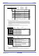
Symbol Address After Reset
UDF 0384
16
00
16
Up/Down Flag
(1)
b7 b6 b5 b4 b3 b2 b1 b0
Bit Name FunctionBit Symbol
0: Down count
1: Up count
TA4P
TA3P
TA2P
Timer A4 up/down flagTA4UD
Timer A3 up/down flagTA3UD
Timer A2 up/down flagTA2UD
Timer A1 up/down flagTA1UD
Timer A0 up/down flagTA0UD
RW
RW
RW
RW
RW
RW
WO
WO
WO
Enabled by setting the MR2 bit in
the TAiMR register to 0
(= switching source in UDF register)
during event counter mode
0: two-phase pulse signal
processing disabled
1: two-phase pulse signal
processing enabled
(2, 3)
Timer A2 two-phase pulse
signal processing select bit
Timer A3 two-phase pulse
signal processing select bit
Timer A4 two-phase pulse
signal processing select bit
NOTES:
1. Use MOV instruction to write to this register.
2. Make sure the port direction bits for the TA2
IN
to TA4I
N
and TA2
OUT
to TA4
OUT
pins are set to 0
input mode.
3. When the two-phase pulse signal processing function is not used, set the corresponding bit to 0.