
Datasheet


12. Timer A
page 103
puorG92/C61M
854fo7002,03.raM21.1.veR
2110-1010B90JER
12.1 Timer A
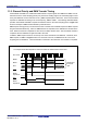
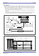
Figure 12.3 shows a block diagram of the timer A. Figures 12.4 to 12.6 show registers related to the timer A.
The timer A supports the following four modes. Except in event counter mode, timers A0 to A4 all have the
same function. Use bits TMOD1 to TMOD0 in the TAiMR register (i = 0 to 4) to select the desired mode.
• Timer mode: The timer counts an internal count source.
• Event counter mode: The timer counts pulses from an external device or overflows and underflows of
other timers.
• One-shot timer mode: The timer outputs a pulse only once before it reaches the minimum count 000016.
• Pulse width modulation (PWM) mode: The timer outputs pulses in a given width successively.
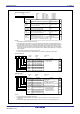
Figure 12.4 TA0MR to TA4MR Registers
Figure 12.3 Timer A Block Diagram
TABSR register
Increment/decrement
TAi
Addresses TAj TAk
Timer A0 0387
16
- 0386
16
Timer A4 Timer A1
Timer A1 0389
16
- 0388
16
Timer A0 Timer A2
Timer A2 038B
16
- 038A
16
Timer A1 Timer A3
Timer A3 038D
16
- 038C
16
Timer A2 Timer A4
Timer A4 038F
16
- 038E
16
Timer A3 Timer A0
Always counts down except
in event counter mode
Reload register
Counter
Low-order
8 bits
High-order
8 bits
Clock source
selection
• Timer
(gate function)
• Timer
• One shot
• PWM
f
1
or f
2
f
8
f
32
TAi
IN
(i = 0 to 4)
TB2 overflow
• Event counter
f
C32
Clock selection
TAj overflow
(j = i – 1. however, j = 4 when i = 0)
Pulse output
Toggle flip-flop
TAi
OUT
(i = 0 to 4)
Data bus low-order bits
Data bus high-order bits
UDF register
Decrement
TAk overflow
(k = i + 1. however, k = 0 when i = 4)
Polarity
selection
To external
trigger circuit
(1)
(1)
NOTE:
1. Overflow or underflow
Clock selection
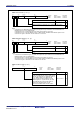
Timer Ai Mode Register (i=0 to 4)
Symbol Address After Reset
TA0MR to TA4MR 0396
16
to 039A
16
00
16
Bit Name FunctionBit Symbol
RW
b7 b6 b5 b4 b3 b2 b1 b0
0 0 : Timer mode
0 1 : Event counter mode
1 0 : One-shot timer mode
1 1 : Pulse width modulation
(PWM) mode
b1 b0
TCK1
MR3
MR2
MR1
TMOD1
MR0
TMOD0
TCK0
Function varies with each
operation mode
Count source select bit
Operation mode select bi
t
RW
RW
RW
RW
RW
RW
RW
RW
Function varies with each
operation mode