
Datasheet

11. DMAC
puorG92/C61M
page 94
854fo7002,03.raM21.1.veR
2110-1010B90JER
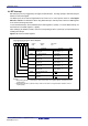
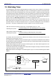
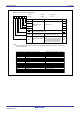
Figure 11.3 DM1SL Register, DM0CON Register, and DM1CON Registers
DMAi Control Register(i=0,1)
Symbol Address After Reset
DM0CON 002C
16 00000X002
DM1CON 003C16 00000X002
Bit Name FunctionBit Symbol
Transfer unit bit select bit
b7 b6 b5 b4 b3 b2 b1 b0
0: 16 bits
1: 8 bits
DMBIT
DMASL
DMAS
DMAE
Repeat transfer mode
select bit
0: Single transfer
1: Repeat transfer
DMA request bit
0: DMA not requested
1: DMA requested
0: Disabled
1: Enabled
0: Fixed
1: Forward
DMA enable bit
Source address direction
select bit
(2)
Destination address
direction select bit
(2)
0: Fixed
1: Forward
DSD
DAD
Nothing is assigned. If necessary, set to 0. When
read, their contents are 0
NOTES:
1. The DMAS bit can be set to 0 by writing 0 by program (This bit remains unchanged even if 1 is written).
2. At least one of bits DAD and DSD must be set to 0 (address direction fixed).
(1)
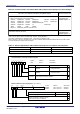
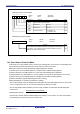
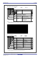
DMA1 Request Cause Select Register
Symbol Address After Reset
DM1SL 03BA
16 0016
Function
Bit Symbol
b7 b6 b5 b4 b3 b2 b1 b0
DMA request cause
select bit
DSEL0
RW
DSEL1
DSEL2
DSEL3
Software DMA
request bit
DSR
DSEL3 to DSEL0
DMS=0(basic cause of request
)
DMS=1(extended cause of request
)
0 0 0 0
2 Falling edge of INT1 pin IC/OC base timer
0 0 0 1
2 Software trigger –
0 0 1 0
2 Timer A0 IC/OC channel 0
0 0 1 1
2 Timer A1 IC/OC channel 1
0 1 0 0
2 Timer A2 –
0 1 0 1
2 Timer A3 SI/O3
0 1 1 0
2 Timer A4 SI/O4
0 1 1 1
2 Timer B0 Two edges of INT1
1 0 0 0
2 Timer B1 –
1 0 0 1
2 Timer B2 –
1 0 1 0
2 UART0 transmit IC/OC channel 2
1 0 1 1
2 UART0 receive IC/OC channel 3
1 1 0 0
2 UART2 transmit IC/OC channel 4
1 1 0 1
2 UART2 receive/ACK2 IC/OC channel 5
1 1 1 0
2 A/D conversion IC/OC channel 6
1 1 1 1
2 UART1 receive IC/OC channel 7
Bit Name
DMA request cause
expansion select bit
DMS
RW
RW
RW
RW
RW
RW
(b5-b4)
RW
RW
RW
RW
RW
RW
RW
(b7-b6)
NOTES:
1. The causes of DMA1 requests can be selected by a combination of DMS bit and bits DSEL3 to DSEL0 in the
manner described below.
Nothing is assigned. If necessary, set
to 0. When read, their contents are 0
A DMA request is generated by
setting this bit to 1 when the DMS bit
is 0 (basic cause) and the DSEL3 to
DSEL0 bits are 0001
2
(software trigger).
The value of this bit when read is 0
0: Basic cause of request
1: Extended cause of request
Refer to note (1)