
Datasheet
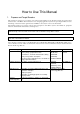
Table Of Contents
- Notes regarding these materials
- General Precautions in the Handling of MPU/MCU Products
- How to Use This Manual
- Table of Contents
- Quick Reference by Address B-
- 1. Overview
- 2. Central Processing Unit (CPU)
- 2.1 Data Registers (R0, R1, R2 and R3)
- 2.2 Address Registers (A0 and A1)
- 2.3 Frame Base Register (FB)
- 2.4 Interrupt Table Register (INTB)
- 2.5 Program Counter (PC)
- 2.6 User Stack Pointer (USP) and Interrupt Stack Pointer (ISP)
- 2.7 Static Base Register (SB)
- 2.8 Flag Register (FLG)
- 2.8.1 Carry Flag (C Flag)
- 2.8.2 Debug Flag (D Flag)
- 2.8.3 Zero Flag (Z Flag)
- 2.8.4 Sign Flag (S Flag)
- 2.8.5 Register Bank Select Flag (B Flag)
- 2.8.6 Overflow Flag (O Flag)
- 2.8.7 Interrupt Enable Flag (I Flag)
- 2.8.8 Stack Pointer Select Flag (U Flag)
- 2.8.9 Processor Interrupt Priority Level (IPL)
- 2.8.10 Reserved Area
- 3. Memory
- 4. Special Function Registers (SFRs)
- 5. Reset
- 6. Processor Mode
- 7. Clock Generation Circuit
- 8. Protection
- 9. Interrupt
- 10. Watchdog Timer
- 11. DMAC
- 12. Timer
- 13. Serial I/O
- 14. A/D Converter
- 15. CRC Calculation Circuit
- 16. Programmable I/O Ports
- 16.1 Port Pi Direction Register (PDi Register, i = 1, 6 to 10)
- 16.2 Port Pi Register (Pi Register, i = 1, 6 to 10)
- 16.3 Pull-up Control Register 0 to Pull-up Control Register 2 (PUR0 to PUR2 Registers)
- 16.4 Port Control Register
- 16.5 Pin Assignment Control register (PACR)
- 16.6 Digital Debounce function
- 17. Flash Memory Version
- 17.1 Flash Memory Performance
- 17.2 Memory Map
- 17.3 Functions To Prevent Flash Memory from Rewriting
- 17.4 CPU Rewrite Mode
- 17.5 Register Description
- 17.6 Precautions in CPU Rewrite Mode
- 17.6.1 Operation Speed
- 17.6.2 Prohibited Instructions
- 17.6.3 Interrupts
- 17.6.4 How to Access
- 17.6.5 Writing in the User ROM Space
- 17.6.6 DMA Transfer
- 17.6.7 Writing Command and Data
- 17.6.8 Wait Mode
- 17.6.9 Stop Mode
- 17.6.10 Low Power Consumption Mode and On-chip Oscillator-Low Power Consumption Mode
- 17.7 Software Commands
- 17.8 Status Register
- 17.9 Standard Serial I/O Mode
- 17.10 Parallel I/O Mode
- 18. Electrical Characteristics
- 19. Usage Notes
- 19.1 SFR
- 19.2 PLL Frequency Synthesizer
- 19.3 Power Control
- 19.4 Protect
- 19.5 Interrupts
- 19.6 DMAC
- 19.7 Timer
- 19.8 Serial I/O
- 19.9 A/D Converter
- 19.10 Programmable I/O Ports
- 19.11 Electric Characteristic Differences Between Mask ROM
- 19.12 Mask ROM Version
- 19.13 Flash Memory Version
- 19.13.1 Functions to Inhibit Rewriting Flash Memory
- 19.13.2 Stop mode
- 19.13.3 Wait mode
- 19.13.4 Low power dissipation mode, on-chip oscillator low power dissipation mode
- 19.13.5 Writing command and data
- 19.13.6 Program Command
- 19.13.7 Operation speed
- 19.13.8 Instructions prohibited in EW0 Mode
- 19.13.9 Interrupts
- 19.13.10 How to access
- 19.13.11 Writing in the user ROM area
- 19.13.12 DMA transfer
- 19.13.13 Regarding Programming/Erasure Times and Execution Time
- 19.13.14 Definition of Programming/Erasure Times
- 19.13.15 Flash Memory Version Electrical Characteristics 10,000 E/W cycle product
- 19.13.16 Boot Mode
- 19.14 Noise
- 19.15 Instruction for a Device Use
- Appendix 1. Package Dimensions
- Appendix 2. Functional Difference
- Register Index
- REVISION HISTORY

General Precautions in the Handling of MPU/MCU Products
The following usage notes are applicable to all MPU/MCU products from Renesas. For detailed usage notes
on the products covered by this manual, refer to the relevant sections of the manual. If the descriptions under
General Precautions in the Handling of MPU/MCU Products and in the body of the manual differ from each
other, the description in the body of the manual takes precedence.
1. Handling of Unused Pins
Handle unused pins in accord with the directions given under Handling of Unused Pins in the
manual.
The input pins of CMOS products are generally in the high-impedance state. In operation
with an unused pin in the open-circuit state, extra electromagnetic noise is induced in the
vicinity of LSI, an associated shoot-through current flows internally, and malfunctions occur
due to the false recognition of the pin state as an input signal become possible. Unused
pins should be handled as described under Handling of Unused Pins in the manual.
2. Processing at Power-on
The state of the product is undefined at the moment when power is supplied.
The states of internal circuits in the LSI are indeterminate and the states of register
settings and pins are undefined at the moment when power is supplied.
In a finished product where the reset signal is applied to the external reset pin, the states
of pins are not guaranteed from the moment when power is supplied until the reset
process is completed.
In a similar way, the states of pins in a product that is reset by an on-chip power-on reset
function are not guaranteed from the moment when power is supplied until the power
reaches the level at which resetting has been specified.
3. Prohibition of Access to Reserved Addresses
Access to reserved addresses is prohibited.
The reserved addresses are provided for the possible future expansion of functions. Do
not access these addresses; the correct operation of LSI is not guaranteed if they are
accessed.
4. Clock Signals
After applying a reset, only release the reset line after the operating clock signal has become
stable. When switching the clock signal during program execution, wait until the target clock
signal has stabilized.
When the clock signal is generated with an external resonator (or from an external
oscillator) during a reset, ensure that the reset line is only released after full stabilization of
the clock signal. Moreover, when switching to a clock signal produced with an external
resonator (or by an external oscillator) while program execution is in progress, wait until
the target clock signal is stable.
5. Differences between Products
Before changing from one product to another, i.e. to one with a different part number, confirm
that the change will not lead to problems.
The characteristics of MPU/MCU in the same group but having different part numbers may
differ because of the differences in internal memory capacity and layout pattern. When
changing to products of different part numbers, implement a system-evaluation test for
each of the products.