
Datasheet
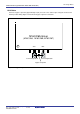
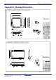
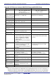

Table Of Contents
- Notes regarding these materials
- General Precautions in the Handling of MPU/MCU Products
- How to Use This Manual
- Table of Contents
- Quick Reference by Address B-
- 1. Overview
- 2. Central Processing Unit (CPU)
- 2.1 Data Registers (R0, R1, R2 and R3)
- 2.2 Address Registers (A0 and A1)
- 2.3 Frame Base Register (FB)
- 2.4 Interrupt Table Register (INTB)
- 2.5 Program Counter (PC)
- 2.6 User Stack Pointer (USP) and Interrupt Stack Pointer (ISP)
- 2.7 Static Base Register (SB)
- 2.8 Flag Register (FLG)
- 2.8.1 Carry Flag (C Flag)
- 2.8.2 Debug Flag (D Flag)
- 2.8.3 Zero Flag (Z Flag)
- 2.8.4 Sign Flag (S Flag)
- 2.8.5 Register Bank Select Flag (B Flag)
- 2.8.6 Overflow Flag (O Flag)
- 2.8.7 Interrupt Enable Flag (I Flag)
- 2.8.8 Stack Pointer Select Flag (U Flag)
- 2.8.9 Processor Interrupt Priority Level (IPL)
- 2.8.10 Reserved Area
- 3. Memory
- 4. Special Function Registers (SFRs)
- 5. Reset
- 6. Processor Mode
- 7. Clock Generation Circuit
- 8. Protection
- 9. Interrupt
- 10. Watchdog Timer
- 11. DMAC
- 12. Timer
- 13. Serial I/O
- 14. A/D Converter
- 15. CRC Calculation Circuit
- 16. Programmable I/O Ports
- 16.1 Port Pi Direction Register (PDi Register, i = 1, 6 to 10)
- 16.2 Port Pi Register (Pi Register, i = 1, 6 to 10)
- 16.3 Pull-up Control Register 0 to Pull-up Control Register 2 (PUR0 to PUR2 Registers)
- 16.4 Port Control Register
- 16.5 Pin Assignment Control register (PACR)
- 16.6 Digital Debounce function
- 17. Flash Memory Version
- 17.1 Flash Memory Performance
- 17.2 Memory Map
- 17.3 Functions To Prevent Flash Memory from Rewriting
- 17.4 CPU Rewrite Mode
- 17.5 Register Description
- 17.6 Precautions in CPU Rewrite Mode
- 17.6.1 Operation Speed
- 17.6.2 Prohibited Instructions
- 17.6.3 Interrupts
- 17.6.4 How to Access
- 17.6.5 Writing in the User ROM Space
- 17.6.6 DMA Transfer
- 17.6.7 Writing Command and Data
- 17.6.8 Wait Mode
- 17.6.9 Stop Mode
- 17.6.10 Low Power Consumption Mode and On-chip Oscillator-Low Power Consumption Mode
- 17.7 Software Commands
- 17.8 Status Register
- 17.9 Standard Serial I/O Mode
- 17.10 Parallel I/O Mode
- 18. Electrical Characteristics
- 19. Usage Notes
- 19.1 SFR
- 19.2 PLL Frequency Synthesizer
- 19.3 Power Control
- 19.4 Protect
- 19.5 Interrupts
- 19.6 DMAC
- 19.7 Timer
- 19.8 Serial I/O
- 19.9 A/D Converter
- 19.10 Programmable I/O Ports
- 19.11 Electric Characteristic Differences Between Mask ROM
- 19.12 Mask ROM Version
- 19.13 Flash Memory Version
- 19.13.1 Functions to Inhibit Rewriting Flash Memory
- 19.13.2 Stop mode
- 19.13.3 Wait mode
- 19.13.4 Low power dissipation mode, on-chip oscillator low power dissipation mode
- 19.13.5 Writing command and data
- 19.13.6 Program Command
- 19.13.7 Operation speed
- 19.13.8 Instructions prohibited in EW0 Mode
- 19.13.9 Interrupts
- 19.13.10 How to access
- 19.13.11 Writing in the user ROM area
- 19.13.12 DMA transfer
- 19.13.13 Regarding Programming/Erasure Times and Execution Time
- 19.13.14 Definition of Programming/Erasure Times
- 19.13.15 Flash Memory Version Electrical Characteristics 10,000 E/W cycle product
- 19.13.16 Boot Mode
- 19.14 Noise
- 19.15 Instruction for a Device Use
- Appendix 1. Package Dimensions
- Appendix 2. Functional Difference
- Register Index
- REVISION HISTORY
Appendix 2. Functional Difference
page 327
923fo7002,51.beF00.2.veR
0020-2020B90JER
)T62/C61M,B62/C61M,A62/C61M(puorGA62/C61M
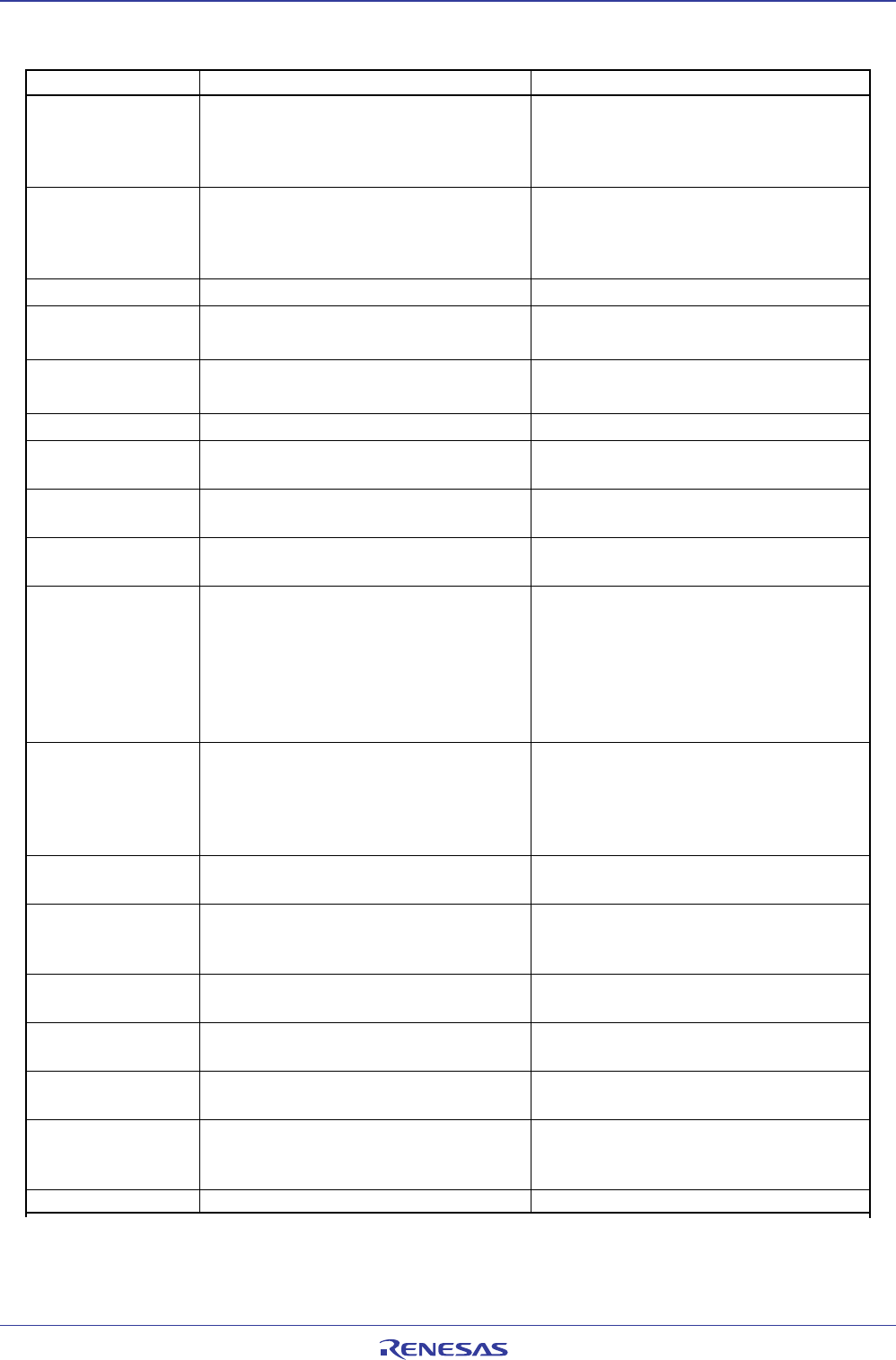
Appendix 2.2 Differences between M16C/26A Group and M16C/26 Group
Item M16C/26A Group M16C/26 Group
Clock Generation 4 circuits (Main clock oscillation circuit, 3 circuits (Main clock oscillation circuit,
Circuit Sub clock oscillation circuit, Sub clock oscillation circuit,
on-chip oscillator, on-chip oscillator)
PLL frequency synthesizer)
System Clock On-chip oscillator Main clock
Source After Reset (Initial value "1" of CM21 bit) (Initial value "0" of CM21 bit)
(Initial value of the CM21
bit in the CM2 register)
On-chip Oscillator Clock
Selectable (8MHz/1MHz/500KHz) Fixed (1MHz)
PACR2 to PACR0 in Necessary to set after reset No PACR register
the PACR register 48pin:"1002", 42pin:"0012"
IFSR20 bit in the Necessary to set to "1" after reset No IFSR2A register
IFSR2A register
External Interrupt
________
8 causes (INT2 added) 7 causes
13 pin
(48-pin version)
________
P84/INT2/ZP IVCC
Function
P70, P71 N-ch open drain output and CMOS N-ch open drain output
output are selectable by S/W
A/D Input Pin 12 channels 8 channels
(48-pin version)
A/D operation Mode 8 modes (single, repeat, single sweep, 5 modes (single, repeat, single sweep,
repeat sweep mode 0, repeat sweep repeat sweep mode 0, repeat sweep
mode 1, simultaneous sampling, mode 1)
delayed trigger mode 0, delayed
trigger mode 1)
1 shunt current measurement function
is available
Timer B Operation 5 modes (timer, event counter, pulse 4 modes (timer, event counter, pulse
Mode periods measurement, pulse width periods measurement, pulse width
measurment, A/D trigger) measurment)
1 shunt current measurement function
is available
CRC Calculation Available (compatible to CRC-CCITT Not available
and CRC-16 methods)
Three-phase motor •Waveform output/Switching port output •Waveform output/Switching port output
Control by software is enabled by software is disabled
•Position data retention function •No position data retention function
Digital Debounce
_______ _____
This function is in the NMI/SD pin and Not available
Function
________
INT5 pin
3 pin
(48-pin version)
P90/CLKOUT/TB0IN/AN30 P90/TB0IN
function (CLKOUT: f1, f8, f32, and fC output)
UART1 Compatible Switching to P64 to P67 or P70 to P73 P64 to P67
pin is enabled
Flash Memory Protection to blocks 0, 1 by FMR02 bit Protection to blocks 0,1 by FMR02 bit
Protect Function Protection to the blocks 0 to 3 by
FMR16 bit
Package
PLQP0048KB-A(48P6Q), PRSP0042GA-B(42P2R)
PLQP0048KB-A(48P6Q)
NOTE:
1. Since the emulator between the M16C/26A Group and M16C/29 Group are the same, all functions of
M16C/29 are built in the emulator. When evaluating M16C/26A Group, do not access to the SFR which
is not built in M16C/26A Group. Refer to Hardware Manual about detail and electrical characteristics.