
Datasheet


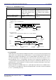

Table Of Contents
- Notes regarding these materials
- General Precautions in the Handling of MPU/MCU Products
- How to Use This Manual
- Table of Contents
- Quick Reference by Address B-
- 1. Overview
- 2. Central Processing Unit (CPU)
- 2.1 Data Registers (R0, R1, R2 and R3)
- 2.2 Address Registers (A0 and A1)
- 2.3 Frame Base Register (FB)
- 2.4 Interrupt Table Register (INTB)
- 2.5 Program Counter (PC)
- 2.6 User Stack Pointer (USP) and Interrupt Stack Pointer (ISP)
- 2.7 Static Base Register (SB)
- 2.8 Flag Register (FLG)
- 2.8.1 Carry Flag (C Flag)
- 2.8.2 Debug Flag (D Flag)
- 2.8.3 Zero Flag (Z Flag)
- 2.8.4 Sign Flag (S Flag)
- 2.8.5 Register Bank Select Flag (B Flag)
- 2.8.6 Overflow Flag (O Flag)
- 2.8.7 Interrupt Enable Flag (I Flag)
- 2.8.8 Stack Pointer Select Flag (U Flag)
- 2.8.9 Processor Interrupt Priority Level (IPL)
- 2.8.10 Reserved Area
- 3. Memory
- 4. Special Function Registers (SFRs)
- 5. Reset
- 6. Processor Mode
- 7. Clock Generation Circuit
- 8. Protection
- 9. Interrupt
- 10. Watchdog Timer
- 11. DMAC
- 12. Timer
- 13. Serial I/O
- 14. A/D Converter
- 15. CRC Calculation Circuit
- 16. Programmable I/O Ports
- 16.1 Port Pi Direction Register (PDi Register, i = 1, 6 to 10)
- 16.2 Port Pi Register (Pi Register, i = 1, 6 to 10)
- 16.3 Pull-up Control Register 0 to Pull-up Control Register 2 (PUR0 to PUR2 Registers)
- 16.4 Port Control Register
- 16.5 Pin Assignment Control register (PACR)
- 16.6 Digital Debounce function
- 17. Flash Memory Version
- 17.1 Flash Memory Performance
- 17.2 Memory Map
- 17.3 Functions To Prevent Flash Memory from Rewriting
- 17.4 CPU Rewrite Mode
- 17.5 Register Description
- 17.6 Precautions in CPU Rewrite Mode
- 17.6.1 Operation Speed
- 17.6.2 Prohibited Instructions
- 17.6.3 Interrupts
- 17.6.4 How to Access
- 17.6.5 Writing in the User ROM Space
- 17.6.6 DMA Transfer
- 17.6.7 Writing Command and Data
- 17.6.8 Wait Mode
- 17.6.9 Stop Mode
- 17.6.10 Low Power Consumption Mode and On-chip Oscillator-Low Power Consumption Mode
- 17.7 Software Commands
- 17.8 Status Register
- 17.9 Standard Serial I/O Mode
- 17.10 Parallel I/O Mode
- 18. Electrical Characteristics
- 19. Usage Notes
- 19.1 SFR
- 19.2 PLL Frequency Synthesizer
- 19.3 Power Control
- 19.4 Protect
- 19.5 Interrupts
- 19.6 DMAC
- 19.7 Timer
- 19.8 Serial I/O
- 19.9 A/D Converter
- 19.10 Programmable I/O Ports
- 19.11 Electric Characteristic Differences Between Mask ROM
- 19.12 Mask ROM Version
- 19.13 Flash Memory Version
- 19.13.1 Functions to Inhibit Rewriting Flash Memory
- 19.13.2 Stop mode
- 19.13.3 Wait mode
- 19.13.4 Low power dissipation mode, on-chip oscillator low power dissipation mode
- 19.13.5 Writing command and data
- 19.13.6 Program Command
- 19.13.7 Operation speed
- 19.13.8 Instructions prohibited in EW0 Mode
- 19.13.9 Interrupts
- 19.13.10 How to access
- 19.13.11 Writing in the user ROM area
- 19.13.12 DMA transfer
- 19.13.13 Regarding Programming/Erasure Times and Execution Time
- 19.13.14 Definition of Programming/Erasure Times
- 19.13.15 Flash Memory Version Electrical Characteristics 10,000 E/W cycle product
- 19.13.16 Boot Mode
- 19.14 Noise
- 19.15 Instruction for a Device Use
- Appendix 1. Package Dimensions
- Appendix 2. Functional Difference
- Register Index
- REVISION HISTORY
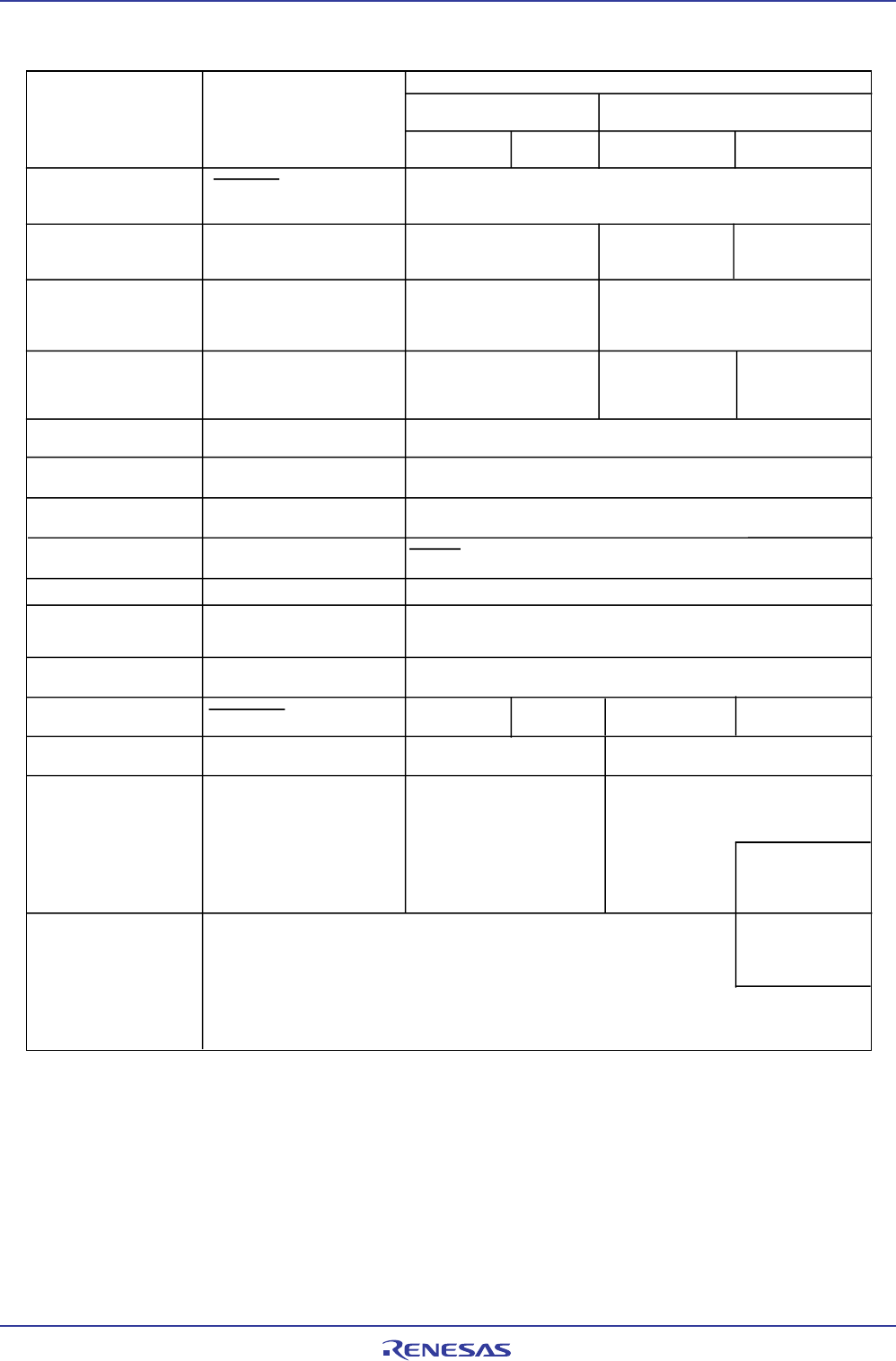
13. Serial I/O
page 162
923fo7002,51.beF00.2.veR
0020-2020B90JER
)T62/C61M,B62/C61M,A62/C61M(puorGA62/C61M
Function
I
2
C bus mode (SMD2 to SMD0 = 0102, IICM = 1)
Clock synchronous serial I/O
mode (SMD2 to SMD0 = 001
2
,
IICM = 0)
Factor of interrupt number
15
(1)
(Refer to Fig.13.1.3.2.)
No acknowledgment
detection (NACK)
Rising edge of SCL
2 9th bit
Factor of interrupt number
16
(1)
1(Refer to Fig.13.1.3.2.)
Start condition detection or stop condition detection
(Refer to Figure 13.1.3.2.1. STSPSEL Bit Function)
UART2 transmission
output delay
Functions of P7
0 pin
Noise filter width
Read RxD2 and SCL
2 pin
levels
Factor of interrupt number
10
(1)
(Refer to Fig.13.1.3.2.)
Acknowledgment detection
(ACK)
Rising edge of SCL
2 9th bit
Initial value of TxD2 and
SDA
2 outputs
UART2 transmission
Transmission started or
completed (selected by U2IRS)
UART2 reception
When 8th bit received
CKPOL = 0 (rising edge)
CKPOL = 1 (falling edge)
Not delayed
TxD2 output
RxD2 input
CLK2 input or output selected
15ns
Possible when the
corresponding port direction bit
= 0
CKPOL = 0 (H)
CKPOL = 1 (L)
Delayed
SDA
2 input/output
SCL
2 input/output
(Cannot be used in I
2
C mode)
Initial and end values of
SCL
2
H
200ns
Always possible no matter how the corresponding port direction bit is set
The value set in the port register before setting I
2
C bus mode
(2)
Timing for transferring data
from the UART reception
shift register to the U2RB
registe
r
IICM2 = 0
(NACK/ACK interrupt)
IICM2 = 1
(UART transmit/ receive interrupt)
CKPH = 1
(Clock delay)
CKPH = 1
(Clock delay)
UART2 transmission
Rising edge of
SCL
2 9th bit
UART2 transmission
Falling edge of SCL
2
next to the 9th bit
UART2 transmission
Falling edge of SCL
2 9th bit
CKPOL = 0 (rising edge)
CKPOL = 1 (falling edge)
Rising edge of SCL
2 9th bit
Falling edge of
SCL
2 9th bit
Falling and rising
edges of SCL
2 9th
bit
DMA1 factor (Refer to Fig.
14.1.3.2.)
UART2 reception
Acknowledgment detection
(ACK)
UART2 reception
Falling edge of SCL
2
9th bi
t
Store received data
1st to 8th bits are stored in
U2RB register bit 0 to bit 7
1st to 8th bits are stored in
U2RB register bit 7 to bit 0
1st to 7th bits are stored in U2RB register
bit 6 to bit 0, with 8th bit stored in U2RB
register bit 8
L
Read U2RB register
Bit 6 to bit 0 as bit 7
to bit 1, and bit 8 as
bit 0
(4)
Read received data
U2RB register status is read
directly as is
CKPH = 0
(No clock delay)
CKPH = 0
(No clock delay)
HL
1st to 8th bits are
stored in U2RB
register bit 7 to bit 0
(3)
Functions of P71 pin
Functions of P7
2 pin
NOTES:
1. If the source or cause of any interrupt is changed, the IR bit in the interrupt control register for the changed interrupt
may inadvertently be set to 1 (interrupt requested). (Refer to “Notes on interrupts” in Usage Notes) If one of the bits
shown below is changed, the interrupt source, the interrupt timing, etc. change. Therefore, always be sure to clear
the IR bit to 0 (interrupt not requested) after changing those bits. SMD2 to SMD0 bits in the U2MR register, IICM bit
in the U2SMR register, IICM2 bit in the U2SMR2 register, CKPH bit in the U2SMR3 register
2. Set the initial value of SDA
2 output while the SMD2 to SMD0 bits in the U2MR register is set to ‘0002’ (serial I/O
disabled).
3. Second data transfer to U2RB register (Rising edge of SCL
2 9th bit)
4. First data transfer to U2RB register (Falling edge of SCL
2 9th bit)
Table 13.1.3.4. I
2
C bus Mode Functions