
Datasheet
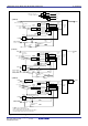
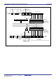
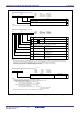
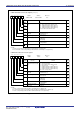

Table Of Contents
- Notes regarding these materials
- General Precautions in the Handling of MPU/MCU Products
- How to Use This Manual
- Table of Contents
- Quick Reference by Address B-
- 1. Overview
- 2. Central Processing Unit (CPU)
- 2.1 Data Registers (R0, R1, R2 and R3)
- 2.2 Address Registers (A0 and A1)
- 2.3 Frame Base Register (FB)
- 2.4 Interrupt Table Register (INTB)
- 2.5 Program Counter (PC)
- 2.6 User Stack Pointer (USP) and Interrupt Stack Pointer (ISP)
- 2.7 Static Base Register (SB)
- 2.8 Flag Register (FLG)
- 2.8.1 Carry Flag (C Flag)
- 2.8.2 Debug Flag (D Flag)
- 2.8.3 Zero Flag (Z Flag)
- 2.8.4 Sign Flag (S Flag)
- 2.8.5 Register Bank Select Flag (B Flag)
- 2.8.6 Overflow Flag (O Flag)
- 2.8.7 Interrupt Enable Flag (I Flag)
- 2.8.8 Stack Pointer Select Flag (U Flag)
- 2.8.9 Processor Interrupt Priority Level (IPL)
- 2.8.10 Reserved Area
- 3. Memory
- 4. Special Function Registers (SFRs)
- 5. Reset
- 6. Processor Mode
- 7. Clock Generation Circuit
- 8. Protection
- 9. Interrupt
- 10. Watchdog Timer
- 11. DMAC
- 12. Timer
- 13. Serial I/O
- 14. A/D Converter
- 15. CRC Calculation Circuit
- 16. Programmable I/O Ports
- 16.1 Port Pi Direction Register (PDi Register, i = 1, 6 to 10)
- 16.2 Port Pi Register (Pi Register, i = 1, 6 to 10)
- 16.3 Pull-up Control Register 0 to Pull-up Control Register 2 (PUR0 to PUR2 Registers)
- 16.4 Port Control Register
- 16.5 Pin Assignment Control register (PACR)
- 16.6 Digital Debounce function
- 17. Flash Memory Version
- 17.1 Flash Memory Performance
- 17.2 Memory Map
- 17.3 Functions To Prevent Flash Memory from Rewriting
- 17.4 CPU Rewrite Mode
- 17.5 Register Description
- 17.6 Precautions in CPU Rewrite Mode
- 17.6.1 Operation Speed
- 17.6.2 Prohibited Instructions
- 17.6.3 Interrupts
- 17.6.4 How to Access
- 17.6.5 Writing in the User ROM Space
- 17.6.6 DMA Transfer
- 17.6.7 Writing Command and Data
- 17.6.8 Wait Mode
- 17.6.9 Stop Mode
- 17.6.10 Low Power Consumption Mode and On-chip Oscillator-Low Power Consumption Mode
- 17.7 Software Commands
- 17.8 Status Register
- 17.9 Standard Serial I/O Mode
- 17.10 Parallel I/O Mode
- 18. Electrical Characteristics
- 19. Usage Notes
- 19.1 SFR
- 19.2 PLL Frequency Synthesizer
- 19.3 Power Control
- 19.4 Protect
- 19.5 Interrupts
- 19.6 DMAC
- 19.7 Timer
- 19.8 Serial I/O
- 19.9 A/D Converter
- 19.10 Programmable I/O Ports
- 19.11 Electric Characteristic Differences Between Mask ROM
- 19.12 Mask ROM Version
- 19.13 Flash Memory Version
- 19.13.1 Functions to Inhibit Rewriting Flash Memory
- 19.13.2 Stop mode
- 19.13.3 Wait mode
- 19.13.4 Low power dissipation mode, on-chip oscillator low power dissipation mode
- 19.13.5 Writing command and data
- 19.13.6 Program Command
- 19.13.7 Operation speed
- 19.13.8 Instructions prohibited in EW0 Mode
- 19.13.9 Interrupts
- 19.13.10 How to access
- 19.13.11 Writing in the user ROM area
- 19.13.12 DMA transfer
- 19.13.13 Regarding Programming/Erasure Times and Execution Time
- 19.13.14 Definition of Programming/Erasure Times
- 19.13.15 Flash Memory Version Electrical Characteristics 10,000 E/W cycle product
- 19.13.16 Boot Mode
- 19.14 Noise
- 19.15 Instruction for a Device Use
- Appendix 1. Package Dimensions
- Appendix 2. Functional Difference
- Register Index
- REVISION HISTORY
13. Serial I/O
page 138
923fo7002,51.beF00.2.veR
0020-2020B90JER
)T62/C61M,B62/C61M,A62/C61M(puorGA62/C61M
Figure 13.1.6. U0C0 to U2C0 registers and UCON register
UARTi Transmit/receive Control Rregister 0 (i=0 to 2)
Symbol Address After Reset
U0C0 to U2C0 03A4
16
, 03AC
16
, 037C
16
00001000
2
b7 b6 b5 b4 b3 b2 b1 b0
Function
TXEPT
CLK1
CLK0
CRS
CRD
NCH
CKPOL
BRG count source
select bit
Transmit register empty
flag
0 : Transmit data is output at falling edge of transfer clock
and receive data is input at rising edge
1 : Transmit data is output at rising edge of transfer clock
and receive data is input at falling edge
CLK polarity select bit
CTS/RTS function
select bit
CTS/RTS disable bi
t
Data output select bit
(5)
0 0 : f
1SIO
or f
2SIO
is selected
0 1 : f
8SIO
is selected
1 0 : f
32SIO
is selected
1 1 : Do not set
b1 b0
0 : LSB first
1 : MSB first
0 : Data in transmit register (during transmission)
1 : No data in transmit register
(transmission completed)
0 : CTS/RTS function enabled
1 : CTS/RTS function disabled
(P6
0
, P6
4
and P7
3
can be used as I/O ports)
(6)
0 : TxDi/SDA2 and SCL2 pins are CMOS output
1 : TxDi/SDA2 and SCL2 pins are N-channel open-drain output
(4)
UFORM Transfer format select bit
(2)
Effective when CRD is set to "0"
0 : CTS function is selected
(1)
1 : RTS function is selected
Bit Name
Bit
Symbol
NOTES:
1. Set the corresponding port direction bit for each CTSi pin to “0” (input mode).
2. Effective when the SMD2 to SMD0 bits in the UMR register to "001
2
"(clock synchronous serial I/O mode) or "010
2
" (UART mode
transfer data 8 bits long). Set the UFORM bit to "1" when the SMD2 to SMD0 bits are set to "101
2
" (I
2
C bus mode) and "0" when
they are set to"100
2
" (UART mode transfer data 7 bits long) or "110
2
" ( UART mode transfer data 9 bits long).
3. CTS
1
/RTS
1
can be used when the CLKMD1 bit in the UCON register is set to “0” (only CLK
1
output) and the RCSP bit in the
UCON register is set to “0” (CTS
0
/RTS
0
not separated).
4. SDA2 and SCL2 are effective when i = 2.
5. When the SMD2 to SMD0 bits in UiMR regiser are set to “000
2
” (serial I/O disable), do not set NCH bit to “1” (TxDi/SDA2 and
SCL2 pins are N-channel open-drain output).
6. When the U1MAP bit in PACR register is “1” (P7
3
to P7
0
), CTS/RTS pin in UART1 is assigned to P7
0
.
7. When the CLK1 and CLK0 bit settings are changed, set the UiBRG register.
RW
RW
RW
RW
RW
RW
RW
RW
RO
(3)
(7)
UART Transmit/receive Control Register 2
Symbol Address After Reset
UCON 03B0
16
X0000000
2
b7 b6 b5 b4 b3 b2 b1 b0
Bit NameBit Symbol RWFunction
CLKMD0
CLKMD1
UART0 transmit interrupt
cause select bit
UART0 continuous
receive mode enable bit
0: Continuous receive mode disabled
1: Continuous receive mode enable
UART1 continuous
receive mode enable bit
UART1 CLK/CLKS
select bit 0
UART1 transmit interrupt
cause select bit
0: Transmit buffer empty (Tl = 1)
1: Transmission completed (TXEPT = 1)
0: Transmit buffer empty (Tl = 1)
1: Transmission completed (TXEPT = 1)
0: Continuous receive mode disabled
1: Continuous receive mode enabled
Nothing is assigned. When write, set to “0”.
When read, the content is indeterminate
U0IRS
U1IRS
U0RRM
U1RRM
UART1 CLK/CLKS
select bit 1
(1)
Effective when CLKMD1 bit is set to “1”
0: Clock output from CLK1
1: Clock output from CLKS1
RCSP
Separate UART0
CTS/RTS bit
(b7)
RW
RW
RW
RW
RW
RW
RW
NOTES:
1. To use more than one transfer clock output pins, set the CKDIR bit in the U1MR register to “0” (internal clock).
2. When the U1MAP bit in PACR register is set to “1” (P7
3
to P7
0
), CTS
0
is supplied from the P7
0
pin.
0: Output from CLK1 only
1: Transfer clock output from multiple
pins function selected
0: CTS/RTS shared pin
1: CTS/RTS separated (CTS
0
supplied
from the P6
4
pin)
(2)