
Datasheet
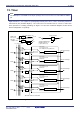
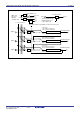

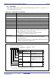
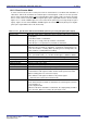
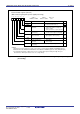
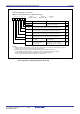
Table Of Contents
- Notes regarding these materials
- General Precautions in the Handling of MPU/MCU Products
- How to Use This Manual
- Table of Contents
- Quick Reference by Address B-
- 1. Overview
- 2. Central Processing Unit (CPU)
- 2.1 Data Registers (R0, R1, R2 and R3)
- 2.2 Address Registers (A0 and A1)
- 2.3 Frame Base Register (FB)
- 2.4 Interrupt Table Register (INTB)
- 2.5 Program Counter (PC)
- 2.6 User Stack Pointer (USP) and Interrupt Stack Pointer (ISP)
- 2.7 Static Base Register (SB)
- 2.8 Flag Register (FLG)
- 2.8.1 Carry Flag (C Flag)
- 2.8.2 Debug Flag (D Flag)
- 2.8.3 Zero Flag (Z Flag)
- 2.8.4 Sign Flag (S Flag)
- 2.8.5 Register Bank Select Flag (B Flag)
- 2.8.6 Overflow Flag (O Flag)
- 2.8.7 Interrupt Enable Flag (I Flag)
- 2.8.8 Stack Pointer Select Flag (U Flag)
- 2.8.9 Processor Interrupt Priority Level (IPL)
- 2.8.10 Reserved Area
- 3. Memory
- 4. Special Function Registers (SFRs)
- 5. Reset
- 6. Processor Mode
- 7. Clock Generation Circuit
- 8. Protection
- 9. Interrupt
- 10. Watchdog Timer
- 11. DMAC
- 12. Timer
- 13. Serial I/O
- 14. A/D Converter
- 15. CRC Calculation Circuit
- 16. Programmable I/O Ports
- 16.1 Port Pi Direction Register (PDi Register, i = 1, 6 to 10)
- 16.2 Port Pi Register (Pi Register, i = 1, 6 to 10)
- 16.3 Pull-up Control Register 0 to Pull-up Control Register 2 (PUR0 to PUR2 Registers)
- 16.4 Port Control Register
- 16.5 Pin Assignment Control register (PACR)
- 16.6 Digital Debounce function
- 17. Flash Memory Version
- 17.1 Flash Memory Performance
- 17.2 Memory Map
- 17.3 Functions To Prevent Flash Memory from Rewriting
- 17.4 CPU Rewrite Mode
- 17.5 Register Description
- 17.6 Precautions in CPU Rewrite Mode
- 17.6.1 Operation Speed
- 17.6.2 Prohibited Instructions
- 17.6.3 Interrupts
- 17.6.4 How to Access
- 17.6.5 Writing in the User ROM Space
- 17.6.6 DMA Transfer
- 17.6.7 Writing Command and Data
- 17.6.8 Wait Mode
- 17.6.9 Stop Mode
- 17.6.10 Low Power Consumption Mode and On-chip Oscillator-Low Power Consumption Mode
- 17.7 Software Commands
- 17.8 Status Register
- 17.9 Standard Serial I/O Mode
- 17.10 Parallel I/O Mode
- 18. Electrical Characteristics
- 19. Usage Notes
- 19.1 SFR
- 19.2 PLL Frequency Synthesizer
- 19.3 Power Control
- 19.4 Protect
- 19.5 Interrupts
- 19.6 DMAC
- 19.7 Timer
- 19.8 Serial I/O
- 19.9 A/D Converter
- 19.10 Programmable I/O Ports
- 19.11 Electric Characteristic Differences Between Mask ROM
- 19.12 Mask ROM Version
- 19.13 Flash Memory Version
- 19.13.1 Functions to Inhibit Rewriting Flash Memory
- 19.13.2 Stop mode
- 19.13.3 Wait mode
- 19.13.4 Low power dissipation mode, on-chip oscillator low power dissipation mode
- 19.13.5 Writing command and data
- 19.13.6 Program Command
- 19.13.7 Operation speed
- 19.13.8 Instructions prohibited in EW0 Mode
- 19.13.9 Interrupts
- 19.13.10 How to access
- 19.13.11 Writing in the user ROM area
- 19.13.12 DMA transfer
- 19.13.13 Regarding Programming/Erasure Times and Execution Time
- 19.13.14 Definition of Programming/Erasure Times
- 19.13.15 Flash Memory Version Electrical Characteristics 10,000 E/W cycle product
- 19.13.16 Boot Mode
- 19.14 Noise
- 19.15 Instruction for a Device Use
- Appendix 1. Package Dimensions
- Appendix 2. Functional Difference
- Register Index
- REVISION HISTORY
12. Timer
page 94
923fo7002,51.beF00.2.veR
0020-2020B90JER
)T62/C61M,B62/C61M,A62/C61M(puorGA62/C61M
12.1 Timer A
Figure 12.1.1 shows a block diagram of the timer A. Figures 12.1.2 to 12.1.4 show registers related to the
timer A.
The timer A supports the following four modes. Except in event counter mode, timers A0 to A4 all have the
same function. Use the TMOD1 to TMOD0 bits in the TAiMR register (i = 0 to 4) to select the desired mode.
• Timer mode: The timer counts an internal count source.
• Event counter mode: The timer counts pulses from an external device or overflows and underflows of
other timers.
• One-shot timer mode: The timer outputs a pulse only once before it reaches the minimum count
“000016.”
• Pulse width modulation (PWM) mode: The timer outputs pulses in a given width successively.
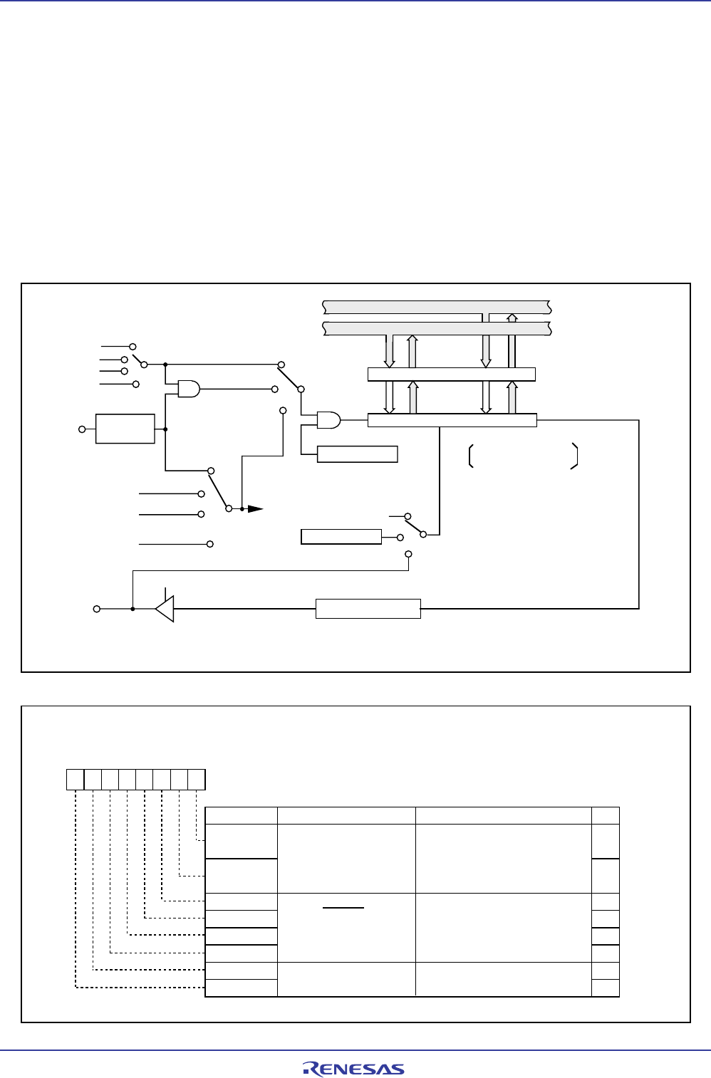
Figure 12.1.2. TA0MR to TA4MR Registers
TABSR register
Up-count/down-count
TAi Addresses TAj TAk
Timer A0 0387
16
- 0386
16
Timer A4 Timer A1
Timer A1 0389
16
- 0388
16
Timer A0 Timer A2
Timer A2 038B
16
- 038A
16
Timer A1 Timer A3
Timer A3 038D
16
- 038C
16
Timer A2 Timer A4
Timer A4 038F
16
- 038E
16
Timer A3 Timer A0
Always counts down except
in event counter mode
Reload register
Counter
Low-order
8 bits
High-order
8 bits
Clock source
selection
• Timer
(gate function)
• Timer
• One shot
• PWM
f
1
or f
2
f
8
f
32
TAi
IN
(i = 0 to 4)
TB2 overflow
• Event counter
f
C32
Clock selection
TAj overflow
(j = i – 1. Note, however, that j = 4 when i = 0)
Pulse output
Toggle flip-flop
TAi
OUT
(i = 0 to 4)
Data bus low-order bits
Data bus high-order bits
UDF register
Down count
TAk overflow
(k = i + 1. Note, however, that k = 0 when i = 4)
Polarity
selection
To external
trigger circuit
(1)
(1)
NOTE:
1. Overflow or underflow
Clock selection
Figure 12.1.1. Timer A Block Diagram
Timer Ai mode register (i=0 to 4)
Symbol Address After reset
TA0MR to TA4MR 0396
16 to 039A16 0016
Bit name FunctionBit symbol
RW
b7 b6 b5 b4 b3 b2 b1 b0
0 0 : Timer mode
0 1 : Event counter mode
1 0 : One-shot timer mode
1 1 : Pulse width modulation
(PWM) mode
b1 b0
TCK1
MR3
MR2
MR1
TMOD1
MR0
TMOD0
TCK0
Function varies with each
operation mode
Count source select bit
Operation mode select bi
t
RW
RW
RW
RW
RW
RW
RW
RW
Function varies with each
operation mode