
Datasheet
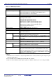
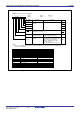
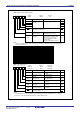
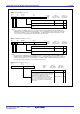
Table Of Contents
- Notes regarding these materials
- General Precautions in the Handling of MPU/MCU Products
- How to Use This Manual
- Table of Contents
- Quick Reference by Address B-
- 1. Overview
- 2. Central Processing Unit (CPU)
- 2.1 Data Registers (R0, R1, R2 and R3)
- 2.2 Address Registers (A0 and A1)
- 2.3 Frame Base Register (FB)
- 2.4 Interrupt Table Register (INTB)
- 2.5 Program Counter (PC)
- 2.6 User Stack Pointer (USP) and Interrupt Stack Pointer (ISP)
- 2.7 Static Base Register (SB)
- 2.8 Flag Register (FLG)
- 2.8.1 Carry Flag (C Flag)
- 2.8.2 Debug Flag (D Flag)
- 2.8.3 Zero Flag (Z Flag)
- 2.8.4 Sign Flag (S Flag)
- 2.8.5 Register Bank Select Flag (B Flag)
- 2.8.6 Overflow Flag (O Flag)
- 2.8.7 Interrupt Enable Flag (I Flag)
- 2.8.8 Stack Pointer Select Flag (U Flag)
- 2.8.9 Processor Interrupt Priority Level (IPL)
- 2.8.10 Reserved Area
- 3. Memory
- 4. Special Function Registers (SFRs)
- 5. Reset
- 6. Processor Mode
- 7. Clock Generation Circuit
- 8. Protection
- 9. Interrupt
- 10. Watchdog Timer
- 11. DMAC
- 12. Timer
- 13. Serial I/O
- 14. A/D Converter
- 15. CRC Calculation Circuit
- 16. Programmable I/O Ports
- 16.1 Port Pi Direction Register (PDi Register, i = 1, 6 to 10)
- 16.2 Port Pi Register (Pi Register, i = 1, 6 to 10)
- 16.3 Pull-up Control Register 0 to Pull-up Control Register 2 (PUR0 to PUR2 Registers)
- 16.4 Port Control Register
- 16.5 Pin Assignment Control register (PACR)
- 16.6 Digital Debounce function
- 17. Flash Memory Version
- 17.1 Flash Memory Performance
- 17.2 Memory Map
- 17.3 Functions To Prevent Flash Memory from Rewriting
- 17.4 CPU Rewrite Mode
- 17.5 Register Description
- 17.6 Precautions in CPU Rewrite Mode
- 17.6.1 Operation Speed
- 17.6.2 Prohibited Instructions
- 17.6.3 Interrupts
- 17.6.4 How to Access
- 17.6.5 Writing in the User ROM Space
- 17.6.6 DMA Transfer
- 17.6.7 Writing Command and Data
- 17.6.8 Wait Mode
- 17.6.9 Stop Mode
- 17.6.10 Low Power Consumption Mode and On-chip Oscillator-Low Power Consumption Mode
- 17.7 Software Commands
- 17.8 Status Register
- 17.9 Standard Serial I/O Mode
- 17.10 Parallel I/O Mode
- 18. Electrical Characteristics
- 19. Usage Notes
- 19.1 SFR
- 19.2 PLL Frequency Synthesizer
- 19.3 Power Control
- 19.4 Protect
- 19.5 Interrupts
- 19.6 DMAC
- 19.7 Timer
- 19.8 Serial I/O
- 19.9 A/D Converter
- 19.10 Programmable I/O Ports
- 19.11 Electric Characteristic Differences Between Mask ROM
- 19.12 Mask ROM Version
- 19.13 Flash Memory Version
- 19.13.1 Functions to Inhibit Rewriting Flash Memory
- 19.13.2 Stop mode
- 19.13.3 Wait mode
- 19.13.4 Low power dissipation mode, on-chip oscillator low power dissipation mode
- 19.13.5 Writing command and data
- 19.13.6 Program Command
- 19.13.7 Operation speed
- 19.13.8 Instructions prohibited in EW0 Mode
- 19.13.9 Interrupts
- 19.13.10 How to access
- 19.13.11 Writing in the user ROM area
- 19.13.12 DMA transfer
- 19.13.13 Regarding Programming/Erasure Times and Execution Time
- 19.13.14 Definition of Programming/Erasure Times
- 19.13.15 Flash Memory Version Electrical Characteristics 10,000 E/W cycle product
- 19.13.16 Boot Mode
- 19.14 Noise
- 19.15 Instruction for a Device Use
- Appendix 1. Package Dimensions
- Appendix 2. Functional Difference
- Register Index
- REVISION HISTORY
11. DMAC
page 86
923fo7002,51.beF00.2.veR
0020-2020B90JER
)T62/C61M,B62/C61M,A62/C61M(puorGA62/C61M
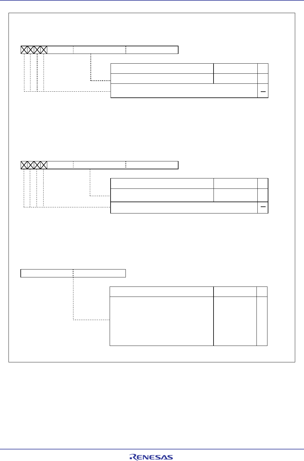
Figure 11.4 SAR0 and SAR1, DAR0 and DAR1, TCR0 and TCR1 Registers
b7 b0 b7 b0
(b8)(b15)
Function
Set the transfer count minus 1. The written value is
stored in the DMAi transfer counter reload register, and
when the DMAE bit in the DMiCON register is set to “1”
(DMA enabled) or the DMAi transfer counter
underflows when the DMASL bit in the DMiCON
register is “1” (repeat transfer), the value of the DMAi
transfer counter reload register is transferred to the
DMAi transfer counter. When read, the DMAi transfer
counter is read.
Symbol Address After reset
TCR0 0029
16
, 0028
16
Indeterminate
TCR1 0039
16
, 0038
16
Indeterminate
DMAi transfer counter (i = 0, 1)
Setting range
0000
16
to FFFF
16
b7
(b23)
b3 b0 b7 b0 b7 b0
(b8)(b16)(b15)(b19)
Function
RW
Set the source address of transfer
Symbol Address After reset
SAR0 0022
16
to 0020
16
Indeterminate
SAR1 0032
16
to 0030
16
Indeterminate
DMAi source pointer (i = 0, 1)
(1)
Setting range
00000
16
to FFFFF
16
Nothing is assigned. When write, set “0”. When read, these contents
are “0”.
Symbol Address After reset
DAR0 0026
16
to 0024
16
Indeterminate
DAR1 0036
16
to 0034
16
Indeterminate
b3 b0 b7 b0 b7 b0
(b8)(b15)(b16)(b19)
Function
Set the destination address of transfer
DMAi destination pointer (i = 0, 1)
(1)
Setting range
00000
16
to FFFFF
16
b7
(b23)
RW
RW
RW
RW
RW
Nothing is assigned. When write, set “0”. When read, these contents
are “0”.
NOTE:
1. If the DSD bit in the DMiCON register is “0” (fixed), this register can only be written to when the DMAE bit in the
DMiCON register is “0” (DMA disabled). If the DSD bit is set to “1” (forward direction), this register can be written to
at any time. If the DSD bit is set to “1” and the DMAE bit is “1” (DMA enabled), the DMAi forward address pointer
can be read from this register. Otherwise, the value written to it can be read.
NOTE:
1. If the DAD bit in the DMiCON register is “0” (fixed), this register can only be written to when the DMAE bit in the
DMiCON register is “0”(DMA disabled). If the DAD bit is set to “1” (forward direction), this register can be written to at
any time. If the DAD bit is set to “1” and the DMAE bit is “1” (DMA enabled), the DMAi forward address pointer can
be read from this register. Otherwise, the value written to it can be read.