
Data Sheet

ICL7106, ICL7107, ICL7107S
FN3082 Rev 9.00 Page 3 of 17
October 24, 2014
Absolute Maximum Ratings Thermal Information
Supply Voltage
ICL7106, V+ to V- . . . . . . . . . . . . . . . . . . . . . . . . . . . . . . . . . . . . . . . . . . 15V
ICL7107, V+ to GND . . . . . . . . . . . . . . . . . . . . . . . . . . . . . . . . . . . . . . . . . 6V
ICL7107, V- to GND. . . . . . . . . . . . . . . . . . . . . . . . . . . . . . . . . . . . . . . . . . -9V
Analog Input Voltage (Either Input) (Note 6
) . . . . . . . . . . . . . . . . . . . V+ to V-
Reference Input Voltage (Either Input). . . . . . . . . . . . . . . . . . . . . . . . V+ to V-
Clock Input
ICL7106 . . . . . . . . . . . . . . . . . . . . . . . . . . . . . . . . . . . . . . . . . . . . TEST to V+
ICL7107 . . . . . . . . . . . . . . . . . . . . . . . . . . . . . . . . . . . . . . . . . . . . .GND to V+
Operating Conditions
Temperature Range . . . . . . . . . . . . . . . . . . . . . . . . . . . . . . . . . 0°C to +70°C
Thermal Resistance (Typical)
JA
(
o
C/W)
PDIP Package (Note 7
) . . . . . . . . . . . . . . . . . . . . . . . . . . 50
MQFP Package (Note 7
) . . . . . . . . . . . . . . . . . . . . . . . . . 75
Maximum Junction Temperature . . . . . . . . . . . . . . . . . . . . . . . . . . . .+150°C
Maximum Storage Temperature Range . . . . . . . . . . . . . .-65°C to +150°C
Pb-Free Reflow Profile (MQFP Package only) . . . . . . . . . . . . . . . see TB493
NOTE: Pb-free PDIPs can be used for through hole wave solder processing
only. They are not intended for use in Reflow solder processing
applications.
CAUTION: Do not operate at or near the maximum ratings listed for extended periods of time. Exposure to such conditions may adversely impact product
reliability and result in failures not covered by warranty.
NOTES:
6. Input voltages may exceed the supply voltages provided the input current is limited to ±100µA.
7.
JA
is measured with the component mounted on a low effective thermal conductivity test board in free air. See Tech Brief TB379 for details.
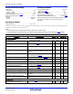
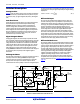
Electrical Specifications (Note 8)
PARAMETER TEST CONDITIONS MIN TYP MAX UNIT
SYSTEM PERFORMANCE
Zero Input Reading V
IN
= 0.0V, full scale = 200mV -000.0 000.0 +000.0 Digital
Reading
Stability (Last Digit) (ICL7107S Only) Fixed input voltage (Note 11
) -000.0 000.0 +000.0 Digital
Reading
Ratiometric Reading V
lN
= V
REF
, V
REF
= 100mV 999 999/1000 1000 Digital
Reading
Rollover Error -V
IN
= +V
lN
200mV
Difference in reading for equal positive and negative inputs
near full scale
- ±0.2 ±1 Counts
Linearity Full scale = 200mV or full scale = 2V maximum deviation
from best straight line fit (Note 10
)
- ±0.2 ±1 Counts
Common Mode Rejection Ratio V
CM
= 1V, V
IN
= 0V, full scale = 200mV (Note 10) - 50 - µV/V
Noise V
IN
= 0V, full scale = 200mV
(peak-to-peak value not exceeded 95% of time)
-15 -µV
Leakage Current Input V
lN
= 0 (Note 10)-110pA
Zero Reading Drift V
lN
= 0, 0°C to +70°C (Note 10) - 0.2 1 µV/°C
Scale Factor Temperature Coefficient V
IN
= 199mV, 0°C to +70°C,
(ext. ref. 0ppm/×°C) (Note 10)
-15ppm/°C
End Power Supply Character V+ Supply Current V
IN
= 0 (does not include LED current for ICL7107) - 1.0 1.8 mA
End Power Supply Character V- Supply Current ICL7107 Only - 0.6 1.8 mA
COMMON Pin Analog Common Voltage 25kΩ between common and positive supply (with respect
to + supply)
2.4 3.0 3.2 V
Temperature Coefficient of Analog Common 25kΩ between common and positive supply (with respect
to + supply)
-80 -ppm/°C
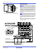
DISPLAY DRIVER ICL7106 ONLY
Peak-to-Peak Segment Drive Voltage
Peak-to-Peak Backplane Drive Voltage
V+ = to V- = 9V (Note 9
) 4 5.5 6 V