
User System Interface Board User's Manual
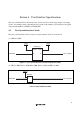
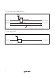
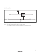
Table Of Contents
- Cover
- Cautions
- IMPORTANT INFORMATION
- SAFETY PAGE
- Preface
- Contents
- Section 1 Configuration
- Section 2 Environmental Conditions
- Section 3 Product Specifications
- Section 4 User Interface Specifications
- Section 5 Connection Procedures
- 5.1 Connecting User System Interface Board to User System
- 5.2 Connecting User System Interface Board to EV-Chip Board
- 5.3 Recommended Dimensions for User System Mount Pad (Footprint)
- 5.4 Dimensions for EV-Chip Board and User System Interface Board
- 5.5 Resulting Dimensions after Connecting User System Interface Board
- Section 6 Installing the MCU to the User System
- Section 7 Verifying Operation
- Section 8 Notice
- Colophon
5
Section 4 User Interface Specifications
The user system interface board incorporates a level conversion circuit supporting a low-voltage
circuit. Accordingly, when connecting the user system to the emulator, pay attention to the signal
delays and the number of FANINs and FANOUTs.
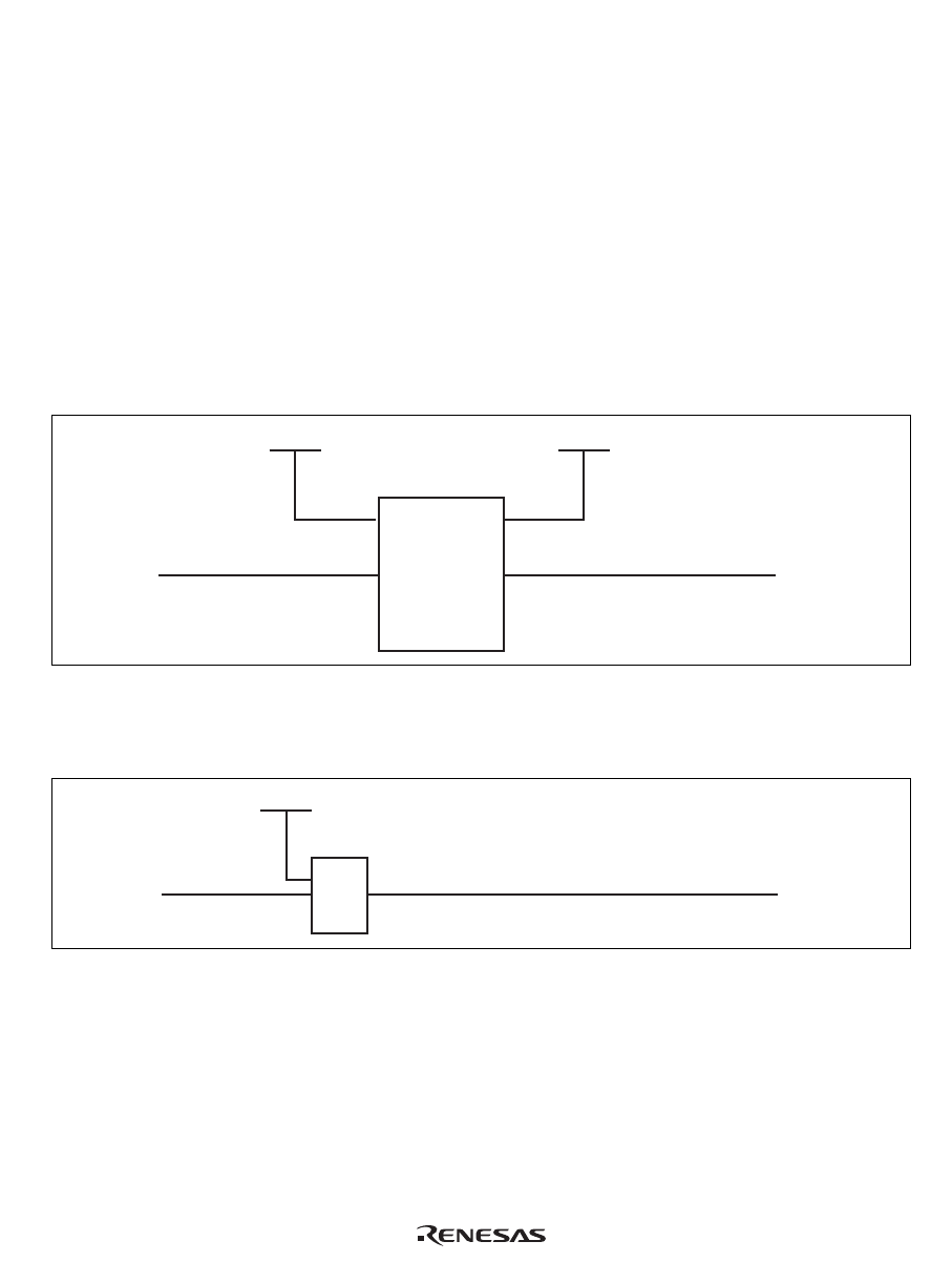
4.1 User System Interface Circuit
The user system interface circuit of the user system interface board is shown below.
(1) NMI and _RES
Emulator User system
HD151015
UVcc
5Vcc
VccB VccA
BA
Figure 3 User System Interface Circuit for NMI and _
RES
(2) PE15 to PE0, PC15 to PC0, PB9 to PB0, PA23 to PA0, and PD31 to PD0
Emulator User system
QS3384
QSVcc
Figure 4 User System Interface Circuit for PE15 to PE0, PC15 to PC0, PB9 to PB0,
PA23 to PA0, and PD31 toPD0