
Datasheet


Section 21 Electrical Characteristics
Rev.5.00 Nov. 02, 2005 Page 327 of 418
REJ09B0028-0500
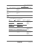
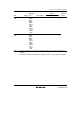
Table 21.5 Serial Communication Interface (SCI) Timing
V
CC
= 3.0 to 5.5 V, V
SS
= 0.0 V, T
a
= –20 to +75°C, unless otherwise indicated.
Applicable
Values
Reference
Item Symbol Pins Test Condition Min Typ Max Unit Figure
Input
clock
Asynchro-
nous
t
Scyc
SCK3 4 — — t
cyc
Figure 21.5
cycle
Clocked
synchro-
nous
6 — —
Input clock pulse
width
t
SCKW
SCK3 0.4 — 0.6 t
Scyc
Transmit data delay t
TXD
TXD V
CC
= 4.0 V to 5.5 V — — 1 t
cyc
Figure 21.6
time (clocked
synchronous)
— — 1
Receive data setup t
RXS
RXD V
CC
= 4.0 V to 5.5 V 50.0 — — ns
time (clocked
synchronous)
100.0 — —
Receive data hold t
RXH
RXD V
CC
= 4.0 V to 5.5 V 50.0 — — ns
time (clocked
synchronous)
100.0 — —