
Datasheet

Section 2 CPU
Rev.5.00 Nov. 02, 2005 Page 43 of 500
REJ09B0027-0500
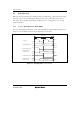
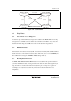
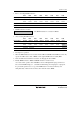
• Prior to executing BSET instruction
P57 P56 P55 P54 P53 P52 P51 P50
Input/output Input Input Output Output Output Output Output Output
Pin state Low
level
High
level
Low
level
Low
level
Low
level
Low
level
Low
level
Low
level
PCR5 0 0 1 1 1 1 1 1
PDR5 1 0 0 0 0 0 0 0
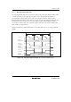
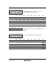
• BSET instruction executed instruction
BSET #0, @PDR5
The BSET instruction is executed for port 5.
• After executing BSET instruction
P57 P56 P55 P54 P53 P52 P51 P50
Input/output Input Input Output Output Output Output Output Output
Pin state Low
level
High
level
Low
level
Low
level
Low
level
Low
level
Low
level
High
level
PCR5 0 0 1 1 1 1 1 1
PDR5 0 1 0 0 0 0 0 1
• Description on operation
1. When the BSET instruction is executed, first the CPU reads port 5.
Since P57 and P56 are input pins, the CPU reads the pin states (low-level and high-level
input).
P55 to P50 are output pins, so the CPU reads the value in PDR5. In this example PDR5 has a
value of H'80, but the value read by the CPU is H'40.
2. Next, the CPU sets bit 0 of the read data to 1, changing the PDR5 data to H'41.
3. Finally, the CPU writes H'41 to PDR5, completing execution of BSET instruction.
As a result of the BSET instruction, bit 0 in PDR5 becomes 1, and P50 outputs a high-level
signal. However, bits 7 and 6 of PDR5 end up with different values. To prevent this problem,
store a copy of the PDR5 data in a work area in memory. Perform the bit manipulation on the
data in the work area, then write this data to PDR5.