
Datasheet

Section 23 Electrical Characteristics
Rev.5.00 Nov. 02, 2005 Page 428 of 500
REJ09B0027-0500
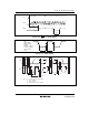
23.3.8 Power-On Reset Circuit Characteristics (Optional)
Table 23.20 Power-On Reset Circuit Characteristics
V
SS
= 0.0 V, T
a
= –20 to +75°C, unless otherwise indicated.
Values
Item Symbol
Test
Condition
Min Typ Max Unit
Pull-up resistance of RES pin R
RES
100 150 — kΩ
Power-on reset start voltage* V
por
— — 100 mV
Note: * The power-supply voltage (Vcc) must fall below Vpor = 100 mV and then rise after
charge of the RES pin is removed completely. In order to remove charge of the RES
pin, it is recommended that the diode be placed in the Vcc side. If the power-supply
voltage (Vcc) rises from the point over 100 mV, a power-on reset may not occur.
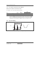
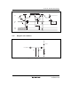
23.4 Operation Timing
t
OSC
V
IH
V
IL
t
CPH
t
CPL
t
CPr
OSC1
t
CPf
Figure 23.1 System Clock Input Timing