
Datasheet


Section 20 Power-On Reset and Low-Voltage Detection Circuits (Optional)
Rev.5.00 Nov. 02, 2005 Page 365 of 500
REJ09B0027-0500
20.3 Operation
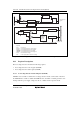
20.3.1 Power-On Reset Circuit
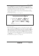
Figure 20.2 shows the timing of the operation of the power-on reset circuit. As the power-supply
voltage rises, the capacitor which is externally connected to the RES pin is gradually charged via
the on-chip pull-up resistor (typ. 150 kΩ). Since the state of the RES pin is transmitted within the
chip, the prescaler S and the entire chip are in their reset states. When the level on the RES pin
reaches the specified value, the prescaler S is released from its reset state and it starts counting.
The OVF signal is generated to release the internal reset signal after the prescaler S has counted
131,072 clock (φ) cycles. The noise cancellation circuit of approximately 100 ns is incorporated to
prevent the incorrect operation of the chip by noise on the RES pin.
To achieve stable operation of this LSI, the power supply needs to rise to its full level and settles
within the specified time. The maximum time required for the power supply to rise and settle after
power has been supplied (t
PWON
) is determined by the oscillation frequency (f
OSC
) and capacitance
which is connected to RES pin (C
RES
). If t
PWON
means the time required to reach 90 % of power
supply voltage, the power supply circuit should be designed to satisfy the following formula.
t
PWON
(ms) ≤ 90 × C
RES
(µF) + 162/f
OSC
(MHz)
(t
PWON
≤ 3000 ms, C
RES
≥ 0.22 µF, and f
OSC
= 10 in 2-MHz to 10-MHz operation)
Note that the power supply voltage (Vcc) must fall below Vpor = 100 mV and rise after charge on
the RES pin is removed. To remove charge on the RES pin, it is recommended that the diode
should be placed near Vcc. If the power supply voltage (Vcc) rises from the point above Vpor, a
power-on reset may not occur.