
Datasheet

Section 17 I
2
C Bus Interface 2 (IIC2)
Rev.5.00 Nov. 02, 2005 Page 329 of 500
REJ09B0027-0500
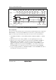
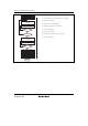
12 781 7812
SCL
MST
TRS
RDRF
ICDRS
ICDRR
SDA
(Input)
Bit 0
Bit 6 Bit 7 Bit 0 Bit 6 Bit 7 Bit 0
Bit 1
User
processing
Data 1
Data 1
Data 2
Data 2
Data 3
[2] Set MST
(when outputting the clock)
[3] Read ICDRR [3] Read ICDRR
Figure 17.15 Receive Mode Operation Timing
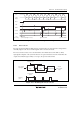
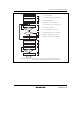
17.4.7 Noise Canceler
The logic levels at the SCL and SDA pins are routed through noise cancelers before being latched
internally. Figure 17.16 shows a block diagram of the noise canceler circuit.
The noise canceler consists of two cascaded latches and a match detector. The SCL (or SDA)
input signal is sampled on the system clock, but is not passed forward to the next circuit unless the
outputs of both latches agree. If they do not agree, the previous value is held.
C
QD
March detector
Internal
SCL or SDA
signal
SCL or SDA
input signal
Sampling
clock
Sampling clock
System clock
period
Latch
Latch
C
Q
D
Figure 17.16 Block Diagram of Noise Conceler