
Datasheet

Section 17 I
2
C Bus Interface 2 (IIC2)
Rev.5.00 Nov. 02, 2005 Page 327 of 500
REJ09B0027-0500
17.4.6 Clocked Synchronous Serial Format
This module can be operated with the clocked synchronous serial format, by setting the FS bit in
SAR to 1. When the MST bit in ICCR1 is 1, the transfer clock output from SCL is selected. When
MST is 0, the external clock input is selected.
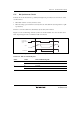
Data Transfer Format
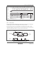
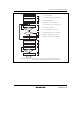
Figure 17.13 shows the clocked synchronous serial transfer format.
The transfer data is output from the rise to the fall of the SCL clock, and the data at the rising edge
of the SCL clock is guaranteed. The MLS bit in ICMR sets the order of data transfer, in either the
MSB first or LSB first. The output level of SDA can be changed during the transfer wait, by the
SDAO bit in ICCR2.
SDA
Bit 0 Bit 1 Bit 2 Bit 3 Bit 4 Bit 5 Bit 6 Bit 7
SCL
Figure 17.13 Clocked Synchronous Serial Transfer Format
Transmit Operation
In transmit mode, transmit data is output from SDA, in synchronization with the fall of the transfer
clock. The transfer clock is output when MST in ICCR1 is 1, and is input when MST is 0. For
transmit mode operation timing, refer to figure 17.14. The transmission procedure and operations
in transmit mode are described below.
1. Set the ICE bit in ICCR1 to 1. Set the MST and CKS3 to CKS0 bits in ICCR1 to 1. (Initial
setting)
2. Set the TRS bit in ICCR1 to select the transmit mode. Then, TDRE in ICSR is set.
3. Confirm that TDRE has been set. Then, write the transmit data to ICDRT. The data is
transferred from ICDRT to ICDRS, and TDRE is set automatically. The continuous
transmission is performed by writing data to ICDRT every time TDRE is set. When changing
from transmit mode to receive mode, clear TRS while TDRE is 1.