
Datasheet

Rev.5.00 Nov. 02, 2005 Page xxix of xxxii
Tables
Section 1 Overview
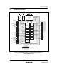
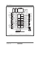
Table 1.1
Pin Functions ............................................................................................................ 7
Section 2 CPU
Table 2.1
Operation Notation ................................................................................................. 22
Table 2.2 Data Transfer Instructions.......................................................................................23
Table 2.3 Arithmetic Operations Instructions (1) ................................................................... 24
Table 2.3 Arithmetic Operations Instructions (2) ................................................................... 25
Table 2.4 Logic Operations Instructions.................................................................................26
Table 2.5 Shift Instructions..................................................................................................... 26
Table 2.6 Bit Manipulation Instructions (1)............................................................................ 27
Table 2.6 Bit Manipulation Instructions (2)............................................................................ 28
Table 2.7 Branch Instructions ................................................................................................. 29
Table 2.8 System Control Instructions.................................................................................... 30
Table 2.9 Block Data Transfer Instructions ............................................................................31
Table 2.10 Addressing Modes ..................................................................................................33
Table 2.11 Absolute Address Access Ranges........................................................................... 35
Table 2.12 Effective Address Calculation (1)........................................................................... 36
Table 2.12 Effective Address Calculation (2)........................................................................... 37
Section 3 Exception Handling
Table 3.1
Exception Sources and Vector Address ..................................................................48
Table 3.2 Interrupt Wait States ............................................................................................... 60
Section 4 Address Break
Table 4.1
Access and Data Bus Used ..................................................................................... 65
Section 5 Clock Pulse Generators
Table 5.1
Crystal Resonator Parameters................................................................................. 71
Section 6 Power-Down Modes
Table 6.1
Operating Frequency and Waiting Time................................................................. 77
Table 6.2 Transition Mode after SLEEP Instruction Execution
and Transition Mode due to Interrupt ..................................................................... 82
Table 6.3 Internal State in Each Operating Mode...................................................................83
Section 7 ROM
Table 7.1
Setting Programming Modes .................................................................................. 95
Table 7.2 Boot Mode Operation ............................................................................................. 97
Table 7.3 System Clock Frequencies for which Automatic Adjustment
of LSI Bit Rate is Possible......................................................................................98