
Datasheet
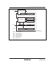

Section 16 Serial Communication Interface 3 (SCI3)
Rev.5.00 Nov. 02, 2005 Page 262 of 500
REJ09B0027-0500
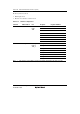
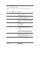
16.2 Input/Output Pins
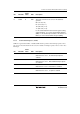
Table 16.2 shows the SCI3 pin configuration.
Table 16.2 Pin Configuration
Pin Name Abbreviation I/O Function
SCI3 clock SCK3 I/O SCI3 clock input/output
SCI3 receive data input RXD Input SCI3 receive data input
SCI3 transmit data output TXD Output SCI3 transmit data output
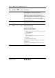
16.3 Register Descriptions
The SCI3 has the following registers for each channel.
• Receive Shift Register (RSR)
• Receive Data Register (RDR)
• Transmit Shift Register (TSR)
• Transmit Data Register (TDR)
• Serial Mode Register (SMR)
• Serial Control Register 3 (SCR3)
• Serial Status Register (SSR)
• Bit Rate Register (BRR)