
Datasheet

Section 15 14-Bit PWM
Rev.5.00 Nov. 02, 2005 Page 256 of 500
REJ09B0027-0500
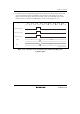
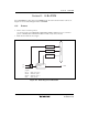
15.2 Input/Output Pin
Table 15.1 shows the 14-bit PWM pin configuration.
Table 15.1 Pin Configuration
Name Abbreviation I/O Function
14-bit PWM square-wave output PWM Output 14-bit PWM square-wave output pin
15.3 Register Descriptions
The 14-bit PWM has the following registers.
• PWM control register (PWCR)
• PWM data register U (PWDRU)
• PWM data register L (PWDRL)
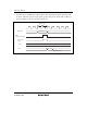
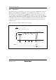
15.3.1 PWM Control Register (PWCR)
PWCR selects the conversion period.
Bit Bit Name
Initial
Value R/W Description
7 to 1 All 1 Reserved
These bits are always read as 1, and cannot be modified.
0 PWCR0 0 R/W Clock Select
0: The input clock is φ/2 (tφ = 2/φ)
The conversion period is 16384/φ, with a minimum
modulation width of 1/φ
1: The input clock is φ/4 (tφ = 4/φ)
The conversion period is 32768/φ, with a minimum
modulation width of 2/φ
Legend: tφ: Period of PWM clock input