
Datasheet

Section 13 Timer Z
Rev.5.00 Nov. 02, 2005 Page 249 of 500
REJ09B0027-0500
8. Notes on Setting Reset Synchronous PWM Mode/Complementary PWM Mode: When bits
CMD1 and CMD0 in TFCR are set, note the following:
A. Write bits CMD1 and CMD0 while TCNT_1 and TCNT_0 are halted.
B. Changing the settings of reset synchronous PWM mode to complementary PWM mode or
vice versa is disabled. Set reset synchronous PWM mode or complementary PWM mode
after the normal operation (bits CMD1 and CMD0 are cleared to 0) has been set.
9. Note on Clearing TSR Flag: When a specific flag in TSR is cleared, a combination of the
BCLR or MOV instructions is used to read 1 from the flag and then write 0 to the flag.
However, if another bit is set during this processing, the bit may also be cleared
simultaneously. To avoid this, the following processing that does not use the BCLR
instruction must be executed. Note that this note is only applied to the F-ZTAT version. This
problem has already been solved in the mask ROM version.
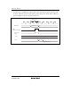
Example: When clearing bit 4 (OVF) in TSR
MOV.B @TSR,R0L
MOV.B #B'11101111, R0L Only the bit to be cleared is 0 and
the other bits are all set to 1.
MOV.B R0L,@TSR
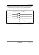
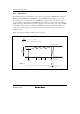
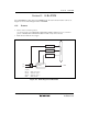
10. Note on Writing to the TOA0 to TOD0 Bits and the TOA1 to TOD1 Bits in TOCR:
The TOA0 to TOD0 bits and the TOA1 to TOD1 bits in TOCR decide the value of the FTIO
pin, which is output until the first compare match occurs. Once a compare match occurs and
this compare match changes the values of FTIOA0 to FTIOD0 and FTIOA1 to FTIOD1
output, the values of the FTIOA0 to FTIOD0 and FTIOA1 to FTIOD1 pin output and the
values read from the TOA0 to TOD0 and TOA1 to TOD1 bits may differ. Moreover, when the
writing to TOCR and the generation of the compare match A0 to D0 and A1 to D1 occur at the
same timing, the writing to TOCR has the priority. Thus, output change due to the compare
match is not reflected to the FTIOA0 to FTIOD0 and FTIOA1 to FTIOD1 pins. Therefore,
when bit manipulation instruction is used to write to TOCR, the values of the FTIOA0 to
FTIOD0 and FTIOA1 to FTIOD1 pin output may result in an unexpected result. When TOCR
is to be written to while compare match is operating, stop the counter once before accessing to
TOCR, read the port 6 state to reflect the values of FTIOA0 to FTIOD0 and FTIOA1 to
FTIOD1 output, to TOA0 to TOD0 and TOA1 to TOD1, and then restart the counter. Figure
13.59 shows an example when the compare match and the bit manipulation instruction to
TOCR occur at the same timing.