
Datasheet

Section 13 Timer Z
Rev.5.00 Nov. 02, 2005 Page 233 of 500
REJ09B0027-0500
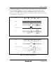
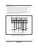
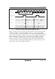
GRA Nn
TCNT
Compare match
signal
Buffer transfer
signal
n
n+1
GRC
N
φ
Figure 13.39 Example of Compare Match Timing for Buffer Operation
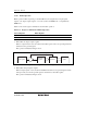
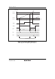
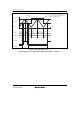
Figure 13.40 shows an operation example in which GRA has been designated as an input capture
register, and buffer operation has been designated for GRA and GRC.
Counter clearing by input capture B has been set for TCNT, and falling edges have been selected
as the FIOCB pin input capture input edge. And both rising and falling edges have been selected
as the FIOCA pin input capture input edge.
As buffer operation has been set, when the TCNT value is stored in GRA upon the occurrence of
input capture A, the value previously stored in GRA is simultaneously transferred to GRC. The
transfer timing is shown in figure 13.41.