
Datasheet

Section 9 I/O Ports
Rev.5.00 Nov. 02, 2005 Page 122 of 500
REJ09B0027-0500
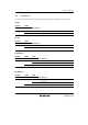
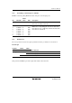
P30 pin
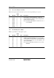
Register PCR3
Bit Name PCR30 Pin Function
Setting Value 0 P30 input pin
1 P30 output pin
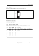
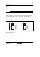
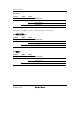
9.4 Port 5
Port 5 is a general I/O port also functioning as an I
2
C bus interface I/O pin, an A/D trigger input
pin, and wakeup interrupt input pin. Each pin of the port 5 is shown in figure 9.4. The register
setting of the I
2
C bus interface register has priority for functions of the pins P57/SCL and
P56/SDA. Since the output buffer for pins P56 and P57 has the NMOS push-pull structure, it
differs from an output buffer with the CMOS structure in the high-level output characteristics (see
section 23, Electrical Characteristics).
P57/SCL
P56/SDA
P55/WKP5/ADTRG
P54/WKP4
P53/WKP3
P52/WKP2
P51/WKP1
P50/WKP0
H8/3687
Port 5
SCL
SDA
P55/WKP5/ADTR
G
P54/WKP4
P53/WKP3
P52/WKP2
P51/WKP1
P50/WKP0
H8/3687N
Port 5
Figure 9.4 Port 5 Pin Configuration
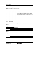
Port 5 has the following registers.
• Port mode register 5 (PMR5)
• Port control register 5 (PCR5)
• Port data register 5 (PDR5)
• Port pull-up control register 5 (PUCR5)