
Datasheet


Section 7 ROM
Rev.5.00 Nov. 02, 2005 Page 92 of 500
REJ09B0027-0500
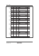
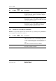
Bit Bit Name
Initial
Value R/W Description
2 PV 0 R/W Program-Verify
When this bit is set to 1, the flash memory changes to
program-verify mode. When it is cleared to 0, program-
verify mode is cancelled.
1 E 0 R/W Erase
When this bit is set to 1 while SWE=1 and ESU=1, the
flash memory changes to erase mode. When it is cleared
to 0, erase mode is cancelled.
0 P 0 R/W Program
When this bit is set to 1 while SWE=1 and PSU=1, the
flash memory changes to program mode. When it is
cleared to 0, program mode is cancelled.
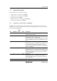
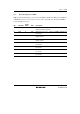
7.2.2 Flash Memory Control Register 2 (FLMCR2)
FLMCR2 is a register that displays the state of flash memory programming/erasing. FLMCR2 is a
read-only register, and should not be written to.
Bit Bit Name
Initial
Value R/W Description
7 FLER 0 R Flash Memory Error
Indicates that an error has occurred during an operation
on flash memory (programming or erasing). When FLER
is set to 1, flash memory goes to the error-protection
state.
See section 7.5.3, Error Protection, for details.
6 to 0 All 0 Reserved
These bits are always read as 0.