
User`s manual


Chapter 4.Board Layout
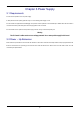
4.1.Component Layout
The following diagram shows top layer component layout of the board.
JA5 JA1
JA6 JA2
J1J3
J2
User LEDs
Power
Application Board
Interface
Microcontroller
Pin Headers
LCD Display
E8 Header
Reset Switch
Potentiometer
User Switches
Boot LED
Power LED
Application Board
Interface
RS2332 Serial
E10A
Debugger
J4
Figure 4-1: Board Layout
7