
Hardware manual


26
In the case of second channel, the situation is little bit different. This is due to the differences in
the architecture of the microcontroller. We can see it very clearly comparing two pictures nr 4-
2.1 and nr 4.2-2. In the first channel we have only four buffer registers and four duty registers
PWDTR1A, PWDTR1C, PWDTR1E and PWDTR1G. In the second channel there are still present
only four buffer registers but there are also all eight duty registers from PWDTR2A till
PWDTR2H. In the first channel so called OTS bit decides to which output data should be
transferred. In the second channel, corresponding bit is called TDS. In this case it decides not to
which output but to which duty register transfer the data. So try to analyze the last picture.
As before at the beginning of PWM period PWM unit checks TDS bit in PWBFR2A and if it is 0
then it transfers data from PWBFR2A to PWDTR2A. If TDS is equal to 1, data from PWBFR2A is
transferred to PWDTR2E. Now, the output of both PWM2A and PWM2E are set to high level and
kept till counter reaches value equal to PWDTR2A or PWDTR2E respectively. Meanwhile we can
put of course new value to PWBFR2A. When the next period starts this new value will be shifted
to proper duty register and the whole process will repeat.
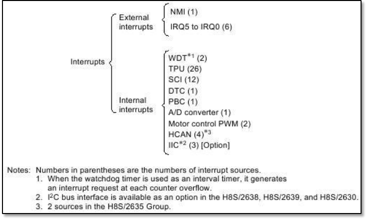
4.3. Interrupts description.
As already mentioned at begin of this chapter there are several sources of interrupts in
H8S/2638. All of them we can separate into external or internal. This separation depends on the
source of the interrupt.
According to the documentation there are seven external interrupts: NMI, IRQ5 to IRQ0 and 49
internal sources of interrupts in the on-chip supporting modules. All available interrupts have its
own address vector and can be seen on the following graph:
Fig. 4.3-1. List of interrupts present in H8S/263* series.