
Hardware manual


Microcomputer Technical Q&A
128
Q&A No.: QAH8S-243
Category: A/D Converter
Subject: Idea Behind External C and R
Question
What is the idea behind the connection of a signal source impedance (tap resistance, etc.) and low-
pass filter to the A/D converter input pins?
Answer
The ideas behind these connections are as follows.
• Permissible signal source impedance
The analog inputs of H8S Series chips are designed so that conversion accuracy is guaranteed
for an input signal with a permissible signal source impedance, R
out
, of 5 k or less (when
φ
>
12 MHz).
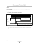
The figure below shows an equivalent circuit of the analog input circuit. In order for A/D
converter to be performed correctly, internal capacitance C
AD
must be charged within the
sampling period, t
SPL
.
Charge time constant τ is expressed as τ = C
AD
× (R
out
+ R
AD
), so that, for a permissible
conversion error of ±4 LSB, for example, the calculation is as follows:
V
CC
× 1020/1024 > V
CC
× (1-exp (–t
SPL
/ τ ))
∴ t
SPL
> 5.6 × τ = 5.6 × C
AD
× (R
out
+ R
AD
)
If t
SPL
= 2 µs (
φ
= 16 MHz, CKS = 1), C
AD
= 20 pF and R
AD
= 10 k ; thus:
τ < 360 ns
∴ R
out
< 8 k