
User`s manual


HokutoElectronic FLASH1 User’s Manual
-6-
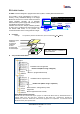
Preparation 1 - Connector & Cable –
FLASH1 Interface Circuit Diagram
Reference Circuit Diagram for Target Board
ILS8P
G1
TXD
RXD
RES
VIN
VPP
MD
G2
1
2
3
4
5
6
7
8
J1
GND
GNDGND
1UF
0.1UF
12KΩ
12KΩ
12KΩ
12KΩ
RESET
RESET
VPP
TXD
RXD
MD
F-ZTAT
CPU
USER VCC
USER VCC
USER VCC
USER VCC
USER VCC
GND
GND
Advice for Making Target Board
1. FLASH1 Vpp electrode capacities are 60mA as maximum.
2.
Please note that MD port
3.
RESET is supposed to be driven with open collector.
Send FLASH1 reset signal to MCU reset port with no delay.
Connect manual RESET with AND parallel circuit or Wired-or.
4.
TXD, RXD must be transmitted at TTL level. RS232C converted signals may be arranged into reverse.
5.
About User VCC
Connector No.5 VIN on programmer side and USERVCC on target board need power supplied to work.
6.
Resistor volume in reference circuit diagram can be adjusted over 10kΩ~47kΩ.
Target board
programming
interface
(8P)
Provided target
cable
FLASH1 programming
interface (10P)
ILS8S
Flash
memory
MCU
Programming
Interface
(8P)
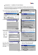
H8/3644F is different at the points below
◆Port name
① PP→P90
② MD→TEST
◆Test port
When programming …High
When executing user program …Low