
Hardware manual


Rev. 3.0, 09/98, page 62 of 361
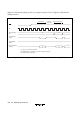
Figure 4.1 indicates the timing of the reset sequence in modes 2 and 3. Figure 4.2 indicates the
timing in mode 1.
Internal address
bus
Internal Read
signal
Internal Write
signal
Internal data bus
(16 bits)
Ø
RES
(2) (3)
(1) (2)
Vector fetch
(1) Reset vector address (H'0000)
(2) Starting address of program (contents of H'0000 to H'0001)
(3) First instruction of program
Instruction prefetch
Internal
processing
Figure 4.1 Reset Sequence (Mode 2 or 3, Program Stored in on-chip ROM)