
Hardware manual


Rev. 3.0, 09/98, page 55 of 361
Bits 6 to 4Standby Timer Select 2 to 0 (STS2 to STS0): These bits select the clock settling
time when the chip recovers from the software standby mode by an external interrupt. During the
selected time the CPU and on-chip supporting modules continue to stand by. These bits should be
set according to the clock frequency so that the settling time is at least 10ms. For specific settings,
see section 14.2, “System Control Register: Power-Down Control Bits.”
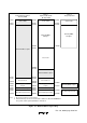
Bit 6
STS2
Bit 5
STS1
Bit 4
STS0 Description
0 0 0 Settling time = 8192 states (Initial value)
0 0 1 Settling time = 16384 states
0 1 0 Settling time = 32768 states
0 1 1 Settling time = 65536 states
1 Settling time = 131072 states
Bit 3Reserved: This bit cannot be modified and is always read as “1.”
Bit 2NMI Edge (NMIEG): Selects the valid edge of the NMI input.
Bit 2
NMIEG Description
0 An interrupt is requested on the falling edge of the NMI input. (Initial value)
1 An interrupt is requested on the rising edge of the NMI input.
Bit 1Dual-Port RAM Mode Enable (DPME): Reserved. Do not write “1” in this bit.
Bit 0RAM Enable (RAME): Enables or disables the on-chip RAM. The RAME bit is
initialized by a reset, but is not initialized in the software standby mode.
Bit 0
RAME Description
0 The on-chip RAM is disabled.
1 The on-chip RAM is enabled. (Initial value)