Hardware manual
Manuals
Brands
Renesas Manuals
Computer Hardware
H8/325 Series
61
62
63
64
65
66
67
68
69
70
Rev. 3.0, 0
9/98, pa
ge 50 of 36
1
Ø
Address bus
AS:
High
RD:
High
WR:
High
Data bus:
high impedance state
Bus cycle
T1 state
T2 state
Address
T3 state
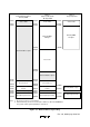
Figure 2.16 Pin States during On-Chip Register Field Access Cycle
1
...
...
59
60
61
62
63
...
...
369