
Hardware manual


Rev. 3.0, 09/98, page 12 of 361
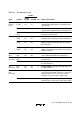
Table 1.3 Pin Functions (cont)
Pin No.
Type Symbol
CG-84
CP-84 FP-80A I/O Name and Function
Bus control WAIT 25 13 I Wait: Requests the CPU to insert TW states
into the bus cycle when an external address is
accessed.
RD 29 17 O Read: Goes Low to indicate that the CPU is
reading an external address.
WR 28 16 O Write: Goes Low to indicate that the CPU is
writing to an external address.
AS 27 15 O Address Strobe: Goes Low to indicate that
there is a valid address on the address bus.
Interrupt
signals
NMI 17 6 I NonMaskable Interrupt: Highest-priority
interrupt request. The NMIEG bit in the system
control register determines whether the
interrupt is requested on the rising or falling
edge of the NMI input.
IRQ
0
to
IRQ
7
30 to 32,
9 to 11,
39, 40
18 to 20,
78 to 80,
27, 28
I Interrupt Request 0 to 7: Maskable interrupt
request pins.
MD
1
,
MD
0
15
16
4
5
I Mode: Input pins for setting the MCU
operating mode according to the table below.
Operating
mode
control
MD
1
MD
0
Mode Description
0 0 Mode 0 Setting prohibited
0 1 Mode 1 Expanded mode with
on-chip ROM disabled
1 0 Mode 2 Expanded mode with
on-chip ROM enabled
1 1 Mode 3 Single-chip mode
These pins must not be changed during MCU
operation.
TxD
0
,
TxD
1
22
9
11
78
O Transmit Data (channels 0 and 1): Data
output pins for the serial communication
interface.
RxD
0
,
RxD
1
21
10
10
79
I Receive Data (channels 0 and 1): Data input
pins for the serial communication interface.
Serial
communi-
cation
interface
SCK
0
,
SCK
1
20
11
9
80
I/O Serial Clock (channels 0 and 1): Input/output
pins for the serial clock.