
Hardware manual


Rev. 3.0, 09/98, page 11 of 361
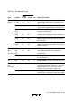
(2) Pin Functions: Table 1.3 gives a concise description of the function of each pin.
Table 1.3 Pin Functions
Pin No.
Type Symbol
CG-84
CP-84 FP-80A I/O Name and Function
Power V
CC
19, 60 8, 47 I Power: Connected to the power supply (+5V).
Connect both VCC pins to the system power
supply (+5V).
V
SS
2, 4, 23,
24, 41,
64, 70
12, 56,
73
I Ground: Connected to ground (0V). Connect
all VSS pins to the system power supply (0V).
Clock XTAL 13 2 I Crystal: Connected to a crystal oscillator. The
crystal frequency should be double the desired
system clock frequency
EXTAL 14 3 I External crystal: Connected to a crystal
oscillator or external clock. The frequency of
the external clock should be double the desired
system clock frequency. See section 15.2,
“Oscillator Circuit,” for examples of connections
to a crystal and external clock.
∅ 26 14 O System clock: Supplies the system clock to
peripheral devices.
RES 12 1 I Reset: A Low input causes the chip to reset.
System
control
STBY 18 7 I Standby: A transition to the hardware standby
mode (a power-down state) occurs when a Low
input is received at the STBY pin.
Address
bus
A
15
to A
0
61 to 63,
65 to 69,
71 to 78
48 to 55,
57 to 64
O Address bus: Address output pins.
Data bus D
7
to D
0
3, 1,
84 to 79
72 to 65 I/O Data bus: 8-Bit bidirectional data bus.